EUV Lithography Makes Good Progress, Still Not Ready for Prime Time
by Anton Shilov on March 10, 2016 3:00 PM EST- Posted in
- Semiconductors
- Intel
- Samsung
- GlobalFoundries
- 15nm
- EUV
- EUVL
- ASML
- TSMC
- 7 nm
At the recent annual SPIE Advanced Lithography conference, Intel, TSMC and other leading semiconductor companies said that significant strides have been made in extreme ultraviolet lithography (EUVL) over the past year or so. Intel did not reveal when exactly it plans to start using EUV technology, but indicated that it will clearly utilize it once it is suitable for high-volume production of semiconductors and is sufficiently cost effective . Samsung and TSMC also intend to start inserting EUVL tools into production in the coming years.
Chip Production Gets Harder
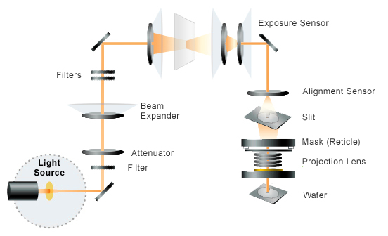
As chipmakers transit to newer process technologies every several years, sizes of transistors and electronic circuits within microprocessors shrink, making them more complex and powerful, but also harder to manufacture using traditional photolithographic methods. Feature sizes of today’s circuits within modern chips can be as small as 42 nm, whereas modern semiconductor production tools use deep ultraviolet (DUV) argon fluoride (ArF) excimer lasers with 193 nm wavelength. To compensate for this difference, Intel and other makers of advanced chips use multiple techniques to enhance resolution of photolithographic equipment.
One of the key transistor density improving technologies is immersion lithography, which replaces the air gap between the lens and wafer with liquid, whose refraction index is higher than one. For example, purified deionized water has refraction index of 1.44 and this allows to enhance resolution of production tools by up to 40% depending on materials. Another key tech for contemporary semiconductor manufacturing is called multiple patterning, a semiconductor production technique that allows to increase feature density by resolving multiple lines on the same photoresist layer using multiple photomasks. Usage of multi-patterning essentially means that certain layers within one chip are exposed multiple times, which greatly increases complexity of manufacturing operations and stretches production cycles, essentially increasing costs of chips.
Intel has been using multi-patterning since mid-2000s and its 65 nm manufacturing technology. The technique did not cause a lot of troubles at first, but things got very complicated with the 14 nm fabrication process because the number of mask steps significantly increased compared to previous-gen technologies. Meanwhile it is taking the company longer to develop its 10 nm manufacturing process, tune its designs and achieve high yields than it used to be, which is why the company had to delay its Cannonlake CPUs from 2016 to 2017. It's also important to note that Intel's 14nm process introduced air gap dielectric in certain interconnect layers, which dramatically increased the number of engineering problems to overcome as introducing voids into the interconnect leads to structural instabilities that must be controlled appropriately.
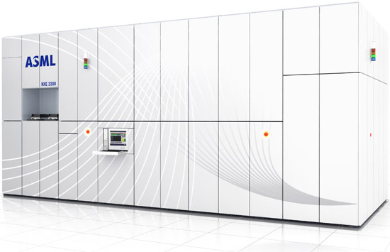
Basically, as it becomes increasingly tougher to develop new manufacturing technologies and produce modern chips using currently available tools, the benefits of node-to-node transitions shrinks, which is rather dangerous for chipmakers from an economic standpoint. In order to address negative effects of multi-patterning, producers of step and scan systems used in semiconductor manufacturing significantly increased output of such tools, as well as enhanced their resolution and boosted their overlay and focus performance. For example, ASM Lithography (ASML), the world’s largest maker of scanners, claims that its latest TWINSCAN NXT:1980Di can process up to 275 wafers per hour and can be used to make chips using sub-10 nm process technologies. While such scanners will be utilized going forward, with so many mask steps required, a new method of photolithography will make far more sense.
EUV Makes a Big Promise, But Generates Big Challenges
EUV lithography, whose development started in 1985 and which used to be called Soft X-Ray, utilizes extreme ultraviolet wavelength of 13.5 nm. Using EUV can greatly enhance the feature density of chips without heavy reliance on multi-patterning and additional layers. For example, TSMC can produce 46 nm metal pitches with a single exposure, an operation that requires usage of four masks for an ArF scanner. Moreover, Intel has managed to produce wafers with 22 nm metal pitches using its own micro EUV tool. Among other advantages, EUV is expected to shrink cycle times and promises to increase yields of chips at advanced nodes. Unfortunately, EUV is an extremely complex technology that not only requires all-new step-and-scan systems for production of semiconductors, new chemicals and new mask infrastructure, but it is also so tricky to use that its actual resolution can end up far below expectations.
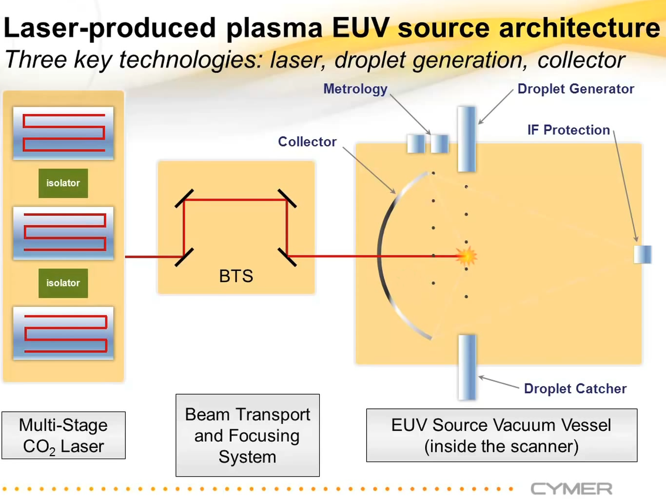
It should be noted that generation of EUV light is a rather difficult process itself. Cymer, a division of ASML that produces light sources for lithography tools, is developing laser produced plasma (LPP) EUV sources. The LPP technology applies CO2 laser to small tin droplets (which are around 30 microns in diameter), creating ionized gas plasma at electron temperatures of several tens of electron volts. The 13.5 nm radiation is then collected by a special ~0.5 meter mirror coated with several layers of molybdenum (Mo) and silicon (Si), in order to selectively reflect the maximum possible amount of 13.5 nm EUV light and direct it to the Intermediate Focus (IF) position at the entrance to the scanner system.
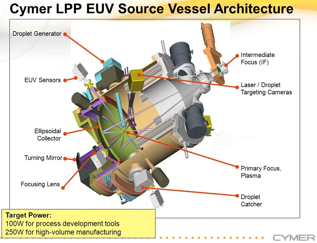
To put it simply: in order to generate 13.5 nm EUV light in a special plasma chamber, you need a very powerful laser (because a significant amount of its power will be wasted); a generator and a catcher for tin droplets (in addition to a debris collector); as well as a special, nearly perfect, elliptical mirror. To make everything even trickier, since EUV light with 13.5 nm wavelength can be absorbed by almost any matter, EUV lithography has to be done in vacuum. This also means that traditional lenses cannot be used with EUV because they absorb 13.5 nm light; instead, specialized multilayer mirrors are used. Even such mirrors absorb about 30% of the light, which is why powerful light sources are needed. This level of absorption can lead to ablative effects on the mirrors themselves, which introduces additional engineering challenges. To learn more how EUV LPP light sources work, check out this video.
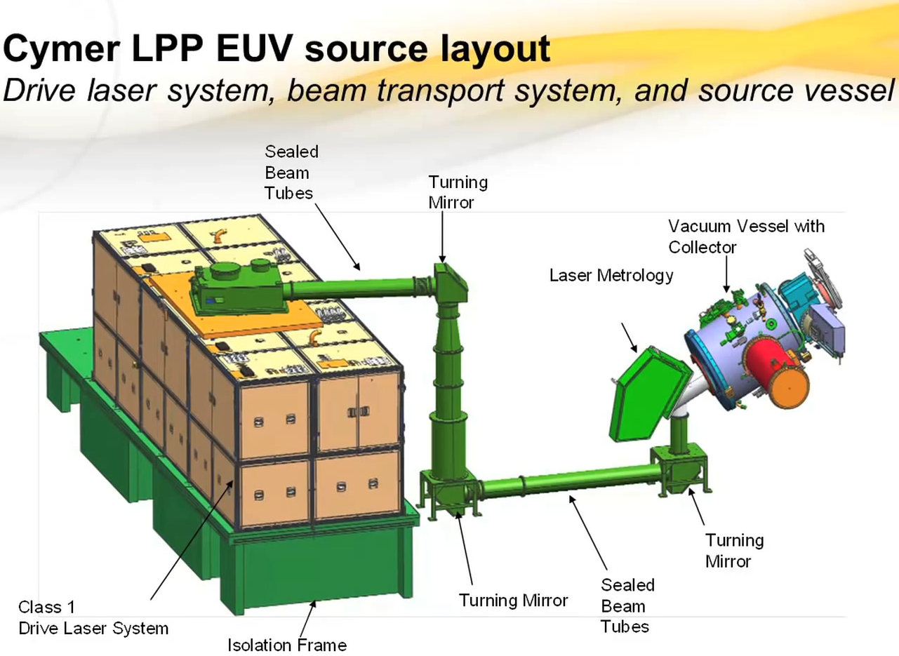
The 13.5 nm EUV light generator needs to have a powerful light source that can expose economically viable amount of wafers per hour (or day). One of the key issues with the TWINCSCAN NXE scanners was that is their laser produced plasma EUV source was not powerful enough. Until recently, performance of experimental EUV equipment from ASML, such as the TWINCSCAN NXE:3300B scanners, was limited to around 500 wafers per day due to power source limitations. By contrast, the current-generation TWINSCAN NXT scanners can process from 175 to 275 wafers per hour (which is good enough, considering heavy usage of multi-patterning). The reliability of the droplet generator was mediocre just about a year ago. Moreover, lifetime of the collector mirror is a yet another point of concern due to the previously mentioned ablative effects.
Things Are Getting Better
The progress of EUVL scanners as well as EUV source systems has been steady in the recent years. ASML, which is one of the major driving forces for extreme ultraviolet lithography, recently said it had hit multiple stability, availability and productivity targets in 2014 and 2015 and is optimistic about the future.
According to ASML, in 2015 one of the company’s clients managed to expose more than 1000 wafers per day on the NXE:3300B, whereas ASML itself managed to hit 1250 wafers per day milestone on the NXE:3350B. ASML also said that it could operate a 200 W light source for one hour with full dose control. For HMV (high volume manufacturing) equipment, 250 W light sources will be needed. ASML is not sure when such light source will be made, but it hopes to hit this milestone in 2016 or 2017. Hence, there is still a long way to go for suitably powerful EUV light sources.
At the SPIE Advanced Lithography conference, Intel confirmed that there were four running EUV tools with 80 W light sources around the world as of early 2016, up from one a year ago. Intel itself now uses the NXE:3300B tool with Cymer’s 80 W EUV sources on its 14 nm pilot line for 21 hours per day, leaving three hours for engineering and servicing. Britt Turkot, senior principal engineer in logic technology development lithography at Intel, said that experimental EUV production had demonstrated good overlay trends, stable critical dimension uniformity as well as good electrical testing and end-of-line yield results.
Another piece of good news is that the reliability of the tin droplet generator also improved significantly over past year. Intel indicated that the tin droplet generator now achieves 85% of its expected lifetime. Reflectivity of the elliptical collector also degrades in accordance with expectations. ASML and Intel are also seeing combined scanner and source availability (4-week rolling average) exceeding 70%, which is good enough for development, but is still unacceptable for mass production. ASML plans to increase availability of its tools to 80% this year.

EUV Photomask Industry Needs Further Development
Extreme ultraviolet lithography no longer uses lenses and traditional glass photomasks (reticles), but utilizes specialized mirrors as well as multi-layer reflective photomasks. Even a minor defect in a photomask makes it unusable because it affects the final wafer. To discover such defects, makers of photomasks or chips can use currently available optical mask inspection tools, e-beam/multi e-beam tools (which are slow) or actinic patterned mask inspection tools, the latter of which have not been commercialized yet. For now, optical mask inspection tools based on 193 nm or other wavelengths can be used for EUV photomasks, but there is a problem.
Since photomasks (reticles) in extreme ultraviolet lithography are even more vulnerable than conventional glass photomasks, they can be easily damaged by falling particles during exposure or even by 13.5 nm EUV light itself. To address this issue, Intel and ASML have been working collaboratively to add a special pellicle to protect the photomask. Protective films for EUV should be extremely thin, should not affect reflection characteristics of photomasks, and should sustain EUV power levels. Unfortunately, it is impossible to use currently available 193 nm mask inspection tools like scanning or tunneling electron microscopes to review an EUV reticle with a pellicle on it, according to SemiEngineering and industry sources. Only actinic patterned mask inspection (APMI) tools are useful for this purpose. However, the latter are not available today outside of academic labs like Berkeley's SHARP mask imaging microscope. As a result, semiconductor companies had to invent a way for mask shops to inspect reticles without pellicles using contemporary equipment and then install protection before shipping masks to fabs (which means that it will be impossible to inspect photomasks after the fact at fabs using current tools). According to the world’s largest CPU maker, its pelliclized reticles can sustain over 200 wafer exposures. However, defectivity levels on such pellicle membranes are still high, which means that flaws can essentially affect wafers and dramatically lower yields. Moreover, it remains to be seen whether producers can supply enough of such membranes.
What is even more important is that to inspect reflective photomasks for EUVL, chipmakers will still need actinic patterned mask inspection equipment. Without such tools and timely repair of photomasks using e-beam tools, yields will inevitably become an issue, Intel has said. Since APMI tools do not exist today (even though KLA-Tencor is said to be developing such devices), it will take years before they reach the market. Moreover, such equipment will not be cheap, they will resemble scanners and will require EUV light sources.
At the SPIE conference, Intel demonstrated successful defect mitigation strategies on multiple devices, and a healthy e-beam pattern defect repair capability. So, the situation with mask inspection and repairs is improving, according to the CPU maker.
EUV Is Required for 7 nm Technology, But Will Be Implemented “When It’s Done”
In general, the industry remains rather optimistic about EUV lithography thanks to two years of solid progress. All leading makers of semiconductors, including Intel, TSMC, Samsung and GlobalFoundries plan to use EUV tools as soon as it makes sense. All four chipmakers indicated on various occasions in the recent months that EUV lithography will be required for 7 nm manufacturing technology. At the SPIE conference, TSMC and Samsung re-affirmed plans to insert EUVL into 7 nm production. By contrast, Intel indicated that while it would prefer to use EUVL for critical layers at 7 nm, it would only use the tech when it is completely ready. At present, Intel is experimenting with EUV on its 14 nm pilot fab line and the results have been encouraging, according to the company. Nonetheless, Intel believes that to make EUV a reality, in addition to many other things, the industry needs to improve yields, decrease costs and develop an ecosystem of EUV photomasks.
Finally, while step-and-scan systems with EUV's 13.5 nm wavelength will help to produce microprocessors and other chips using 5 nm and, perhaps, 7nm, technologies, contemporary 193nm ArF tools are not going anywhere. Virtually all chipmakers say that EUV scanners will only be used for critical layers of chips. For layers that can be produced using multi-patterning, DUV tools will be used.
Intel, TSMC and Samsung have publicly said that they plan to start producing chips using their 10 nm manufacturing technologies in 2017. These process technologies have already been developed without EUV, and unless the chipmakers decide to introduce new versions that involve EUV for critical layers, EUV will continue to not be used for 10 nm. The leading makers of semiconductors are currently finalizing their 7 nm technologies this year, and they will have to make decisions regarding usage of EUV tools with their 7 nm nodes in 2018 – 2019, according to Peter Wennink, CEO of ASML. If currently available EUV tools meet expectations of chipmakers, they will order production TWINSCAN NXE systems and will use them two or three years down the road.
Sources: Intel, Semiconductor Engineering, Semiconductor Manufacturing and Design, SemiWiki.
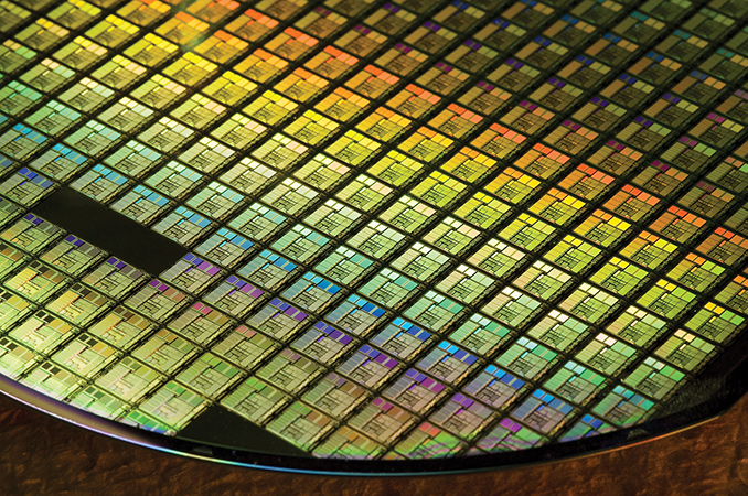
Images courtesy of ASML, Cymer, TSMC.


38 Comments
View All Comments
alyarb - Thursday, March 10, 2016 - link
EUV still not ready, and you HEARD IT FIRST ON ANANDTECH, hahMondozai - Thursday, March 10, 2016 - link
Great, intelligent retort to this article. Just go away if you're not going to engage in substance.prisonerX - Friday, March 11, 2016 - link
Welcome to the internet, I hope you enjoy your stay,lol
boeush - Thursday, March 10, 2016 - link
The complexity, novelty, and wear characterustucs of the tin droplet EUV source make me wonder why they aren't just going with a synchrotron instead - a well-studied, mature tech that can produce very well-behaved, high-power, and highly wavelength/polarization-tunable beams (and doesn't require a hyper-precise collector mirror that must be frequently replaced)...jann5s - Thursday, March 10, 2016 - link
It's because of the wavelength, synchrotrons produce mostly x-Ray's by bending the path of electrons. Those X-rays are useful for imaging because the pass easily through matter without affecting it too much. In lithography you need Ray's that affect your material to produce a big enough change to allow selective etching.boeush - Thursday, March 10, 2016 - link
Not really. I was speaking more broadly of synchrotron radiation - not just ring accelerators in particular (which incidentally emit broad spectrum, not just x-rays). For instance, a linac feeding into a wiggler array can efficiently produce highly tuned, narrow-band emission centered around virtually any wavelength you want (you just tweak various design parameters accordingly.)Vatharian - Friday, March 11, 2016 - link
AFAIK synchrotrons can't produce light longer than 1nm, which bounds them as pure X-ray sources. To reliably manipulate anything, 6-7 nm would be required, enabling ~2-2.5 nm element size. That's the hard limit before switching to direct nanoscale manipulation. X-ray has to be skipped entirely. This article show that we have 30-40 years worth of photolitography development ahead of us. After this, either we must develop high volume electron manipulation processes. Alternative is to either switch to another material that will allow to be easily patterned, or introduce room-temperature superconductors to chips, which will allow to scale back a little on process, by limiting current leaks.Arnulf - Friday, March 11, 2016 - link
"and doesn't require a hyper-precise collector mirror that must be frequently replaced"You cannot do away with these mirrors. They replace lenses and you would have no way of focusing the beam without them.
And unless they invent mirrors with better reflectivity at these wavelengths ablation will always take place and mirrors will have to be replaced after certain period of usage.
tygrus - Sunday, March 13, 2016 - link
Focus doesn't matter if you block rays that are not going the right direction. Not matter which ways you do it, EUV lithography will waste more power (produce more heat) and be very costly to use. There is 1 layer of transistors (that may require a few masks and developing/processing) on top of that are metal layers. First the small and short close to the transistors then the fat wide ones on top for power buses and longer wires. The fat/wide wires don't need EUV. Bottom few layers will use EUV.nandnandnand - Thursday, March 10, 2016 - link
"will help to produce microprocessors and other chips using 5 nm and, perhaps, 7nm, technologies"Switch 5 nm and 7 nm.