Samsung Begins Mass Production Of 96L 3D NAND
by Billy Tallis on July 9, 2018 11:00 PM EST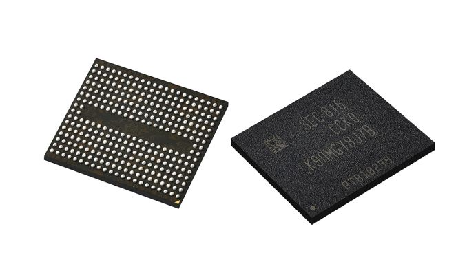
Samsung has started mass production of their fifth generation of 3D NAND flash memory, which they brand as V-NAND. This new generation bumps the layer count from 64 up to 96 (officially, "more than 90" layers), providing further density increases without incurring the endurance and reliability costs that came with process shrinks for planar NAND flash memory. Samsung first announced their 96L V-NAND at Flash Memory Summit in August 2017.
The fifth generation V-NAND also includes performance enhancements, most significantly a Toggle DDR 4.0 interface running at 1.4Gbps, compared to the 800Mbps interface speed of Samsung's previous 3D NAND. A reduction of operating voltage from 1.8V to 1.2V offsets the extra power consumption that faster interface speed would otherwise bring. Samsung is also citing improvements to both read and program latency. Read latency did not improve from 48L to 64L, but now has been "significantly" reduced to 50μs. Program (write) latency is down about 30% to 500μs.
Samsung hasn't shared many details about their process refinements, but the height of each memory cell layer has been reduced by 20%, which helps reduce the extremely high aspect ratio of the holes that need to be etched for the vertical strings of memory cells. Difficulties with high aspect ratio etching are widely believed to be the primary cause for delays that Samsung's 48L V-NAND suffered, which led to several product cancellations as Samsung's NAND development failed to keep pace with their SSD controller improvements. Samsung's transition to 64 layers was much smoother, and Samsung is claiming a 30% improvement to manufacturing productivity with the 96L process. Whether this is on a per-bit basis or a per-wafer basis, this should allow for another on-time roll out.
The first 96L part in mass production is a 256Gb TLC (three bits per cell) die, which should see broad usage in the mobile and SSD markets. Larger dies will follow to fulfill the need for higher capacities with lower cost per bit, primarily in the enterprise SSD market. This will include a 1Tb QLC NAND (four bits per cell) part.
Source: Samsung


25 Comments
View All Comments
GTRagnarok - Tuesday, July 10, 2018 - link
Will 3D NAND keep getting more layers for try foreseeable future? Is there a limit?GTRagnarok - Tuesday, July 10, 2018 - link
*thehaukionkannel - Wednesday, July 11, 2018 - link
A kind of limit... the higher stack, the more wiring is needed to connect those stacks. Also the heat may become more problematic in lower part of the stack. But the wiring is the Main problem. Aka you need to have electronic router from each stack to each other stack and that Number increases when you make higher stacks.FullmetalTitan - Thursday, July 12, 2018 - link
There is a limit based on the current string stacking and cell design. Several companies expect to be able to hit 128 layers on their current technologies, but several are investigating new cell designs and layer topologies to move beyond 128L NAND.tommo1982 - Friday, July 13, 2018 - link
Is TLC the only one affected with reliability issues when shrinking the process or does it affect SLC and MLC as well?