Western Digital Begins to Sample QLC BiCS4: 1.33 Tbit 96-Layer 3D NAND
by Anton Shilov on July 20, 2018 2:00 PM EST
Western Digital has started sampling its 96-layer 3D NAND chips featuring QLC architecture that stores four bits per cell. The chip happens to be the world’s highest-capacity 3D NAND device. The company expects to commence volume shipments of this memory chip already this calendar year.
Western Digital’s 96-layer BICS4 3D QLC NAND chip can store up to 1.33 Tb of raw data, or around 166 GB. The IC will be initially used for consumer products Western Digital sells under the SanDisk brand, so think of memory cards (e.g., high-capacity SD and microSD products), USB drives, and some other devices. The manufacturer expects its 3D QLD NAND memory to be used in a variety of applications, including retail, mobile, embedded, client, and enterprise, but does not elaborate on timing at this point.
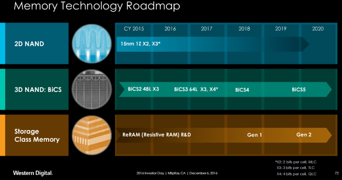
The 1.33-Tb BICS4 IC is Western Digital’s second-gen 3D QLC NAND device. Last year the company announced its BICS3 64-layer 3D QLC chips featuring a 768 Gb capacity, but it is unclear whether they have ever been used for commercial products. Meanwhile, it is clear that the device was used to learn about 3D QLC behavior in general (i.e., endurance, read errors, retention, etc.)
Western Digital and its manufacturing partner Toshiba started volume production of 96-layer 3D NAND earlier this year. Western Digital confirmed in late May that it had begun volume shipments of its BiCS4 memory to its retail customers, which most probably means that the new 96-layer 3D NAND ICs were used for select SanDisk-branded products. The first BiCS4 products that Western Digital announced were 256 Gb 3D TLC ICs, so it is highly likely that they have been in mass production for some time now.
As it appears, yields of 96-layer 3D NAND have been good enoug,h and things that the company has learned with BiCS3 QLC were substantial, so Western Digital moved right to its top-of-the-range capacity of 1.33 Tb per chip. What is noteworthy is that officially the BiCS4 range was to include both TLC and QLC ICs with capacities ranging from 256 Gb to 1 Tb, so the 1.33 Tb IC is a surprising addition to the lineup which signals Western Digital’s confidence of its technology.
Related Reading
- Western Digital Announce BiCS4 3D NAND: 96 Layers, TLC & QLC, Up to 1 Tb per Chip
- Western Digital: 96-Layer 3D NAND Progressing Well, Shipping to Retail Customers
- Western Digital Announces Four Bit Per Cell 64-Layer 3D NAND Flash
- Intel Teases Upcoming QLC SSD For Datacenters
- Samsung Begins Mass Production Of 96L 3D NAND
- We Found a Prototype 4 TB Intel QLC SSD
- Intel QLC NAND Updates: Up to 20TB In 2.5-inch SSD
- Intel And Micron Launch First QLC NAND: Micron 5210 ION Enterprise SATA SSD
Source: Western Digital


40 Comments
View All Comments
Oxford Guy - Saturday, July 21, 2018 - link
Drive death is not the only issue. Steady state performance for the original 120 GB 840 drive was horrendous, as documented at hardocpCheapSushi - Saturday, July 21, 2018 - link
Yeah, cost, size and total drive endurance, not cell endurance. Hard to believe enthusiasts are so bad at understanding said products.porcupineLTD - Sunday, July 22, 2018 - link
Lets use an example:Kingston SSDNow G2 240GB planar MLC - 300 TBW
Kingston A1000 240GB 3D TLC - 150 TBW
That looks to me like half the endurance when 3D TLC was supposed to have similar endurance to planar MLC, actualy if you look you will notice that manufacturers no longer provide TBW instead providing the more ambiguous and arbitrary MTBF (the reason I use Kingston drives as an example is because they still provide TBW) so there goes drive endurance.
As for cost, memory companies already have huge margins (Samsung approaching 75%) so most of the cost of the drives is from the profit the companies make not from the cost of making the NAND (they just want spend even less which is normal for for profit companies but that doesn't mean consumers should swallow their bullshit marketing) so there goes cost.
As for size that is the only somewhat good point, however size can be reduced by 33% just by going from 64L to 96L witch it did and could continue to do (dont know for how long) without sacrificing endurance, but Samsung sells 2TB single sided m2 drives so at least in the consumer space size does not seem to be a problem.
But hey, that's just my limited understanding based of my amateur observations, maybe a true enthusiast like yourself could shed some light on my unfounded concerns.
porcupineLTD - Sunday, July 22, 2018 - link
Edit: the TBW should be measured in TBAlso more examples:
Samsung 860 EVO 250GB TBW -150 TB MTBF - 1.500k h
Samsung 960 EVO 250GB TBW -100 TB MTBF - 1.500k h
Notice how the endurance went down between generations (I'm assuming because of a smaller node) but MTBF remained the same? :)
Bulat Ziganshin - Saturday, July 21, 2018 - link
with SLC->QLC transition capacity grows only linearly, while endurance fails exponentially. SLC had 100K cycles, while TLC with the same error-correction algos had only 500 cyclesit's pure math - with N bits per cell, you have only N times more capacity, but need to distinguish 2^N signal levels which, all things being equal, require to have 2^N bigger cell
CheapSushi - Saturday, July 21, 2018 - link
1000 cycles actuallyerple2 - Sunday, July 22, 2018 - link
That doesn't seem right. 2 bits per cell means you can store 4 pieces of info, instead of 2. At 3 bits per cell, it's 8 unique values per cell. at 4 bits per cell, it's 16 unique values. So QLC is, for the same physical size, 16x more dense.Back in the day, you could get a X-25E 32-ish gig drive that had roughly 100,000 P/E cycles. I don't know where you can buy SLC-only devices today. Nowadays, you can get a 2-4ishTB drive with only 1000 P/E cycles (about 50x-100x-ish the size). Given the relative size of the drive, the TBW is reasonably in the same ballpark, so I would expect endurance, as per measured in bytes written, to be the same order of magnitude. Given that several studies have suggested that the biggest limiting factor in drive replacement isn't really endurance failure, but other factors, it doesn't sound to me like fancy expensive high-endurance-on-a-per-cell basis is all that important.
porcupineLTD - Sunday, July 22, 2018 - link
TBW:Micron P300 200GB planar SLC - 3.5 Petabytes
Samsung 960 EVO 250GB 3D TLC - 100 Terabytes
The only reason for the reduced TBW was the small capacity, bigger capacity would stack with the superior endurance of SLC.
close - Sunday, July 22, 2018 - link
@bcronce, I perfectly agree that the SSD has a chance to fail for multiple other resins then failing cells. As I said in my previous comment I noticed this myself, albeit on a much smaller sample than Google's.But the fact that the SSDs might fail after the same TBW doesn't lead to the conclusion that MLC, TLC, and QLC have the same endurance but rather that SSD (as in the entire usint) tends to fail before you reach any of those limits.
A QLC cell will fail faster than a MLC all other things identical. It's physics. You can mitigate it with better error recovery algorithms, more spare space, bigger cell and manufacturing process but in the end it will still fail faster.
"Luckily" you might not notice because the rest of the SSD will give up before that. :)
DeepLake - Friday, July 20, 2018 - link
They may go bigger node for sure. They are saving alot by going 96L, they may aswell lose some by going larger node, maybe still pulling ahead a little in the end. Maybe yields are also abit higher than smaller node's. On the other hand QLC had issues with P/E voltage so they might benefit from smaller node. We can just speculate, im sure they are doing very well :D