Intel: EUV-Enabled 7nm Process Tech is on Track
by Anton Shilov on December 6, 2018 10:00 AM EST- Posted in
- Semiconductors
- CPUs
- Intel
- 10nm
- EUV
- 7nm
- Manufacturing
Originally planned to enter mass production in the second half of 2016, Intel’s 10 nm process technology is still barely used by the company today. Currently the process is used to produce just a handful of CPUs, ahead of an expected ramp to high-volume manufacturing (HVM) only later in 2019. Without a doubt, Intel suffered delays on its 10 nm process by several years, significantly impacting the company's product lineup and its business.
Now, as it turns out, Intel’s 10 nm may be a short-living node as the company’s 7 nm tech is on-track for introduction in accordance with its original schedule.
For a number of times Intel said that it set too aggressive scaling/transistor density targets for its 10 nm fabrication process, which is why its development ran into problems. Intel’s 10 nm manufacturing tech relies exclusively on deep ultraviolet lithography (DUVL) with lasers operating on a 193 nm wavelength. To enable the fine feature sizes that Intel set out to achieve on 10 nm, the process had to make heavy usage of mutli-patterning. According to Intel, a problem of the process was precisely its heavy usage of multipatterning (quad-patterning to be more exact).
By contrast, Intel’s 7 nm production tech will use extreme ultraviolet lithography (EUVL) with laser wavelength of 13.5 nm for select layers, reducing use of multipatterning for certain metal layers and therefore simplifying production and shortening cycle times. As it appears, the 7 nm fabrication process had been in development separately from the 10 nm tech and by a different team. As a result, its development is well underway and is projected to enter HVM in accordance with Intel’s unannounced roadmap, the company says.
Murthy Renduchintala, chief engineering officer and president of technology, systems architecture and client group at Intel is quoted to have said at the Nasdaq's 39th Investor Conference:
“7 nm for us is a separate team and largely a separate effort. We are quite pleased with our progress on 7 nm. In fact, very pleased with our progress on 7 nm. I think that we have taken a lot of lessons out of the 10 nm experience as we defined that and defined a different optimization point between transistor density, power and performance and schedule predictability. […] So, we are very, very focused on getting 7 nm out according to our original internal plans.”
The Intel exec reaffirmed the company plans to start HVM production of client CPUs using its 10 nm process technology in 2019, with datacenter products following on a bit later. That said, Intel is clearly not skipping any of its already announced 10 nm products, but implies that its 7 nm products may hit the market earlier than we might expect today (i.e., four years after the 10 nm).
“One thing I will say is that as you look at 7 nm, for us this is really now a point in time where we will get EUV back into the manufacturing matrix, and therefore, I think, that will give us a degree of back to the traditional Moore’s Law cadence that we were really talking about,”
“[With 7 nm] we are going back to more like a 2X scaling factor […] and then really moving forward with that goal.”
Intel has never disclosed characteristics of its 7 nm fabrication tech, but a major reduction of multi-patterning usage as well as a more traditional 2X scaling goal vs. 10 nm indicates a more extensive usage of EUVL.
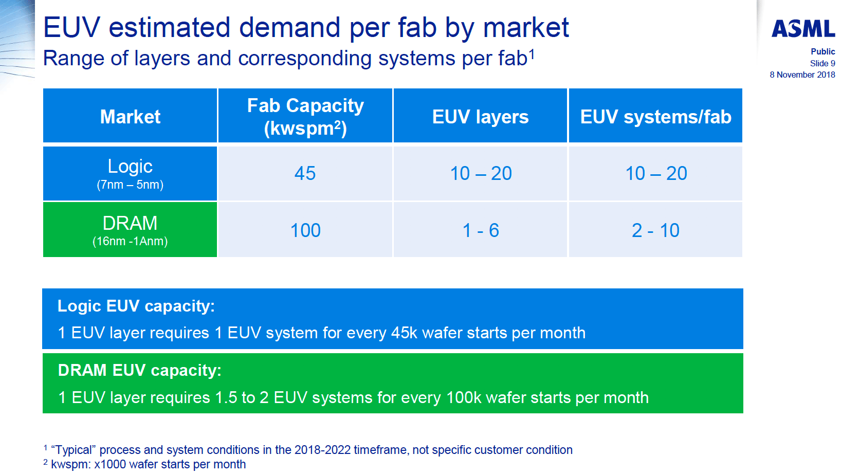
According to ASML, one EUV layer requires one EUV step-and-scan system for every ~45,000 wafer starts per month. Therefore, if Intel plans to use EUVL extensively for 10 to 20 layers, it will require approximately 20 to 40 EUVL scanners for a fab with a 100,000 wafer starts per month capacity. Considering that Intel is not the only company with plans to use EUVL in the 2020s, getting the number of EUVL scanners it might need for HVM at multiple fabs may be a challenge.
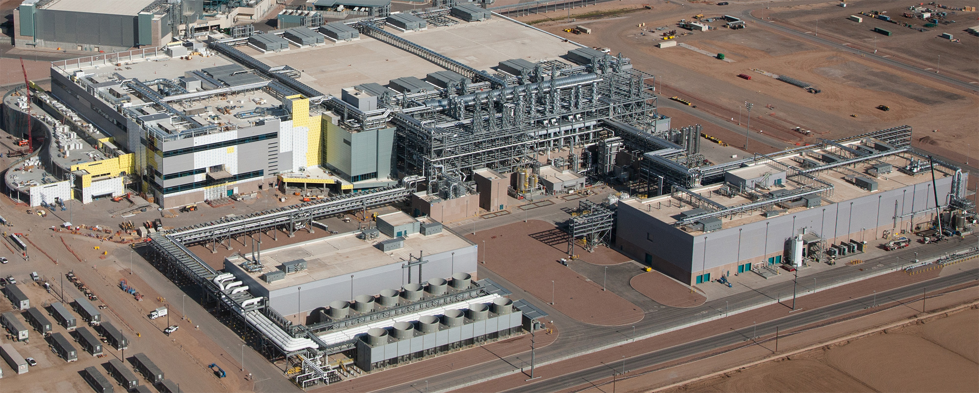
Meanwhile, so far Intel has announced plans for only one 7 nm fab: the Fab 42 in Arizona. In addition, the company is going to have some 7 nm-capable capacity at its D1 facility used for development and trials (among other things).
Related Reading:
- Intel to Equip Fab 42 for 7 nm
- Intel Discloses Plans to Spend $5 Billion on Fab 28 Expansion in Israel
- Intel 10 nm Production Update: Systems on Shelves For Holiday 2019
- Intel’s Xeon Scalable Roadmap Leaks: Cooper Lake-SP, Ice Lake-SP Due in 2020
- Samsung Starts Mass Production of Chips Using Its 7 nm EUV Process Tech
- TSMC: First 7 nm EUV Chips Taped Out, 5 nm Risk Production in Q2 2019
- Samsung Foundry Updates: 8LPU Added, EUVL on Track for HVM in 2019
- ASML Ships Twinscan NXT:2000i Scanner for 7 nm and 5 nm DUV
- EUV Lithography Makes Good Progress, Still Not Ready for Prime Time
Sources: Intel, SeekingAlpha


79 Comments
View All Comments
PeachNCream - Thursday, December 6, 2018 - link
Sunflower!HStewart - Thursday, December 6, 2018 - link
Manufacturing plant FAB 42 in Chandler, Arizona!sing_electric - Thursday, December 6, 2018 - link
It's interesting that Intel is blaming its 10nm issues on SAQP, since TSMC's 7nm process also uses SAQP and they seemingly haven't had the issues with yields that Intel has, since they're shipping in bulk to Apple, MediaTek and others.Intel's publicly said that they expect their 1st gen 10nm process to be lower-performing than 14nm++ (part of the reason that their first 10nm chip out was an i3 instead of an i7 or something). At the time, they said they expected 10nm+ to finally be faster. I wonder how many "10nm+" features they've been able to bake in to the 1st gen tech while they've been trying to increase yields - if it's not many, then it looks like 10nm may be a short-lived node indeed, with AMD nipping at Intel's heels on performance (again, assuming 10nm isn't a performance increase over what we're seeing now).
edzieba - Thursday, December 6, 2018 - link
That was definitely an eyebrow-raiser, the introduction of the Cobalt was generally taken as the big speed bump. Either they're playing "don't mention the war!", Or they may be switching from from Cobalt back to Copper for 7nm.HStewart - Thursday, December 6, 2018 - link
Where do you see them blaming it on SAQP.We are talking about Node process - actually CPU functionality should not be related - fox example AVX 512 and other enhancements.
I believe 7nm - just allows it to have more logic and run at higher speeds and lower power.
iwod - Thursday, December 6, 2018 - link
>Where do you see them blaming it on SAQP.It is written in the article.
FreckledTrout - Friday, December 7, 2018 - link
If you read between the lines from what all Intel has said over the last year I think this sums up the issues. Intel tried to go to dense with 10nm using SAQP which at the end of the day needed use EUV as the quad patterning just isn't as precise EUV. This is exactly why TSMC is successful because even their 7nm is slightly less dense than Intel's original plan for 10nm. once Intel is up on 7nm EUV I suspect they will be back in the lead for densities but honestly at this point it doesn't matter as there is a whole lot more to improve until a completely new way of creating chips occurs.davidefreeman - Thursday, December 6, 2018 - link
If this comment holds true, Intel is in terrible, unless it means for years after the +planned+ launch of 10nm.implies that its 7nm products may hit the market earlier than we might expect today (i.e., four years after the 10nm).
Poik - Thursday, December 6, 2018 - link
My interpretation is the 7nm timeline hast changed. They figured they would have 4 years at 10nm and then transition to 7nm in year 5. Year 5 is looking to hold true, but the 10nm timeline is becoming shorter and shorter as time moves forward.PeachNCream - Thursday, December 6, 2018 - link
That is similar to the impression I got. It seems as though 10nm delays are not impacting anything but 10nm production. 7nm was planned for year x and will likely go into production at the intended time.