Examining Intel's Ice Lake Processors: Taking a Bite of the Sunny Cove Microarchitecture
by Dr. Ian Cutress on July 30, 2019 9:30 AM EST- Posted in
- CPUs
- Intel
- 10nm
- Microarchitecture
- Ice Lake
- Project Athena
- Sunny Cove
- Gen11
Intel has been building up this year to its eventual release of its first widely available consumer 10nm Core processor, codenamed "Ice Lake". The new SoC has an improved CPU core, a lot more die area dedicated to graphics, and is designed to be found in premium notebooks from major partners by the end of 2019, just in time for Christmas. With the new CPU core, Sunny Cove, Intel is promoting a clock-for-clock 18% performance improvement over the original Skylake design, and its Gen11 graphics is the first 1 teraFLOP single SoC graphics design. Intel spent some time with us to talk about what’s new in Ice Lake, as well as the product's direction.
The Core of Core: 10th Gen Core
Intel’s first batch of 10nm Ice Lake processors are being given the official brand name of ‘Intel 10th Generation Core’, and will feature up to four cores with hyperthreading and up to 64 execution units of Gen11 graphics. The aim of this first round of parts will be the thin-and-light mobile market in the form of the Ice Lake-U and Ice Lake-Y processors. Intel uses these designation for anything from 5W to 28W TDP, which covers all the mobile ultra-premium devices.
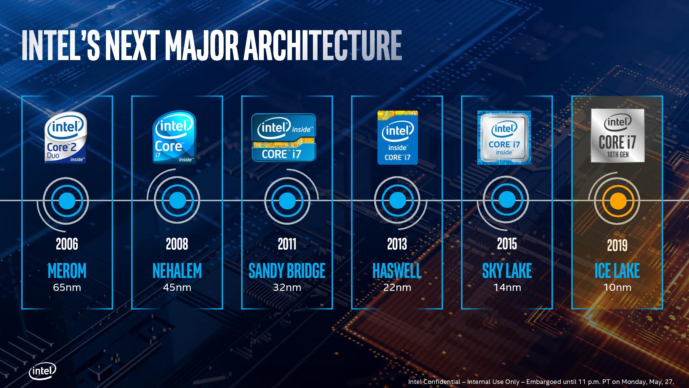
The cores inside Ice Lake-U are based on the ‘Sunny Cove’ microarchitecture, and are a further extension of the overall Core microarchitecture design. The new core affords several security benefits towards Spectre and Meltdown, and Intel is promoting a very healthy 18% IPC increase from its Skylake microarchitecture, which was initially launched as a 6th Gen Core part in 2015 (more on this later).
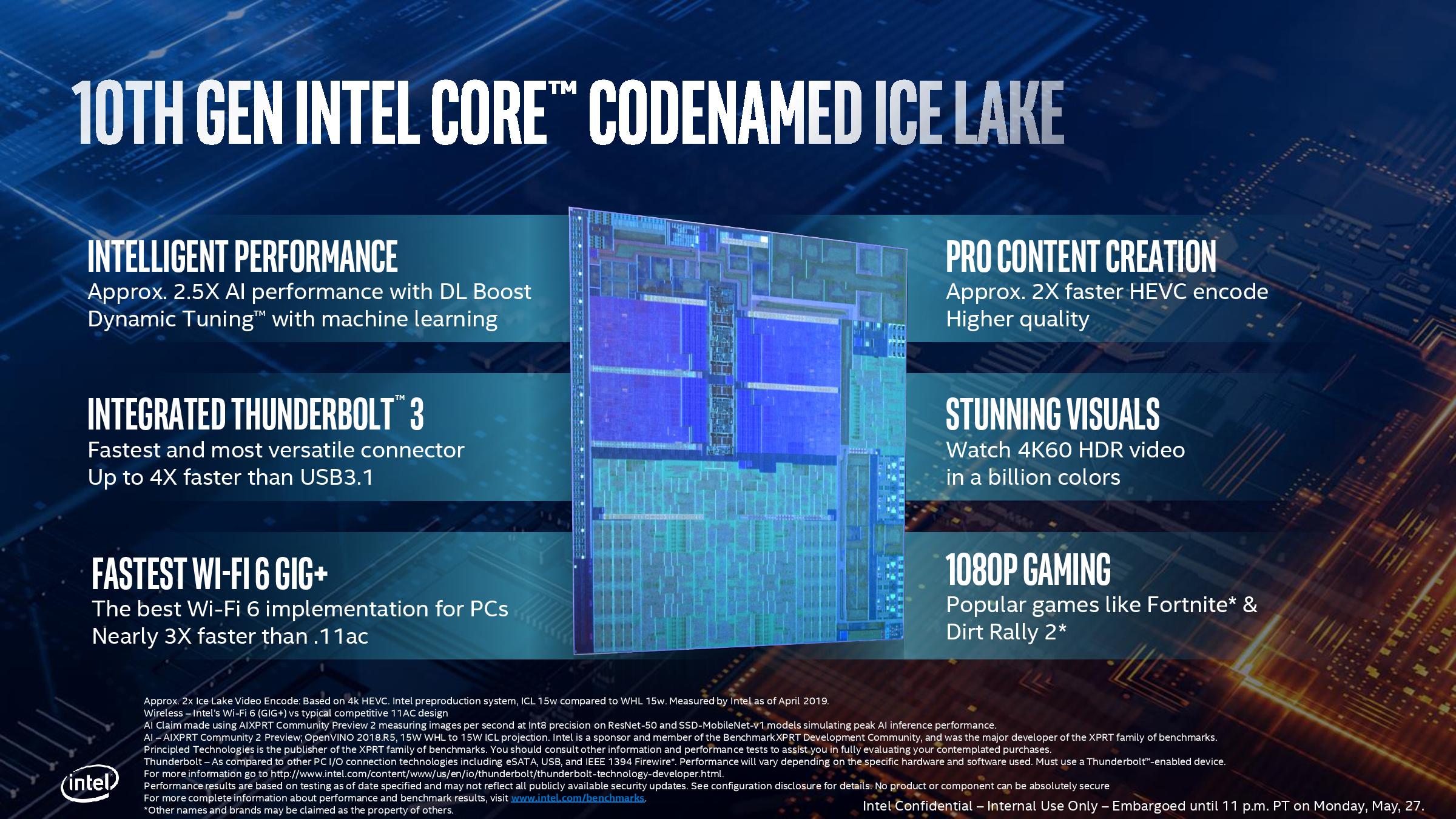
Asides from the core design, and the increased graphics performance, Intel is also putting a lot of effort into the rest of the design of the SoC. This includes AVX-512 extensions to help with deep learning and inference (applying pre-trained neural networks to new situations), integrated Thunderbolt 3 support for up to four full-bandwidth ports, CNVi support for Wi-Fi 6, and a range of platform designs under the umbrella of Intel’s new Project Athena initiative, which Intel hopes to spur on the next generation of premium devices and experiences in this market.
The Processors
Despite Intel continually talking about upcoming devices, and very general top down specifications, we have not seen a full, official CPU list from the company about what frequencies and what performance metrics the new Ice Lake processors will have. At an event a couple of months back, Intel showed this slide:
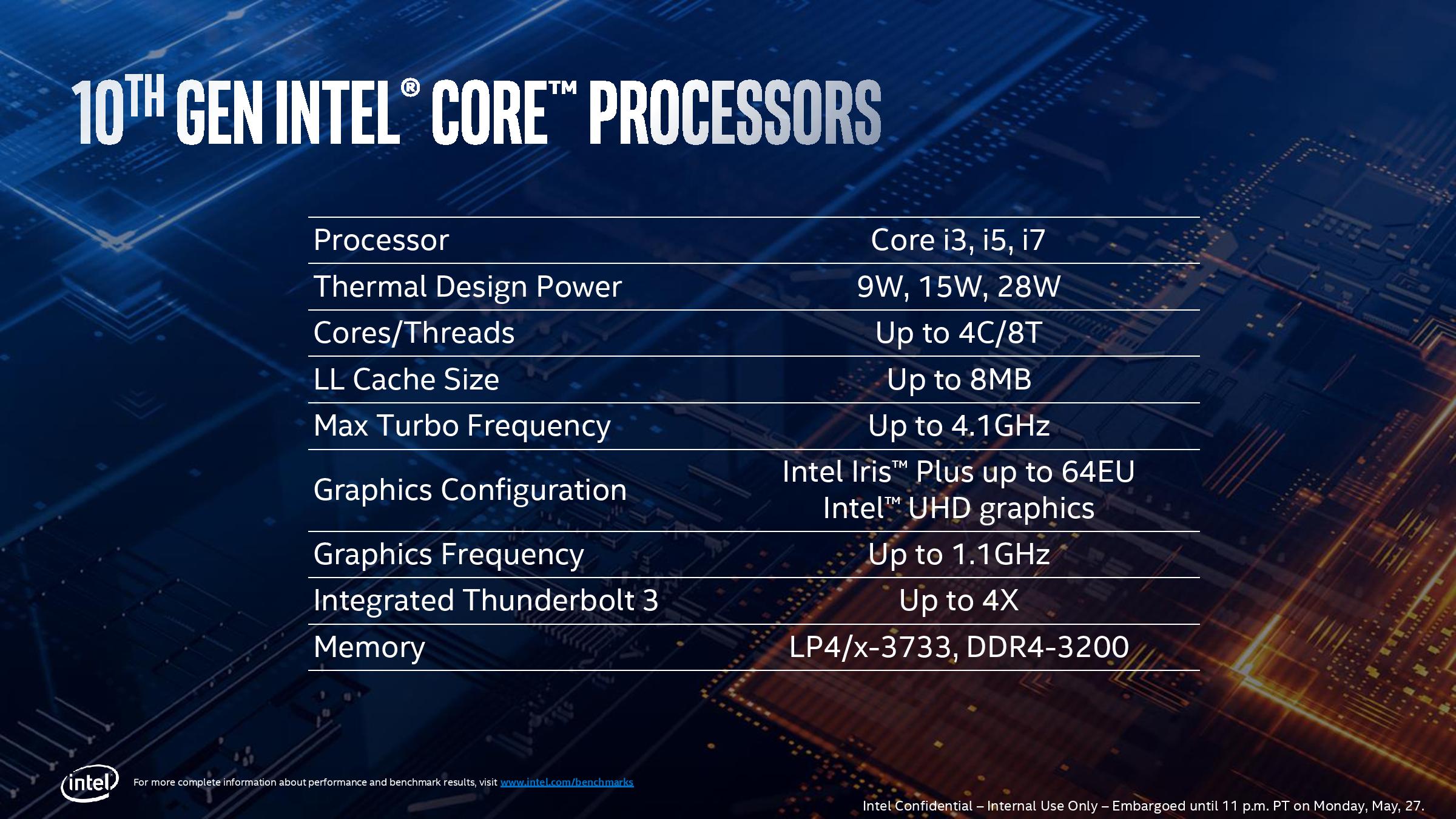
This slide states that we should expect to see i3, i5, and i7 versions of Ice Lake, with TDPs ranging from 9W to 28W, however the key value in there would be 15W. The processors will be up to four cores (so expect to see some dual cores), with a turbo frequency up to 4.1 GHz. Graphics will be available up to 64 execution units and up to 1.1 GHz, with certain platforms enabling four Thunderbolt 3 ports. Memory gets a healthy boost compared to previous platforms, with support being up to LPDDR4X-3733 (32 GB) or DDR4-3200 (64 GB). Each CPU has 16 PCIe 3.0 lanes for external use, although there are actually 32 in the design but 16 of these are tied up with Thunderbolt support.
Without a specific CPU list, it becomes a little worrying that the company hasn’t actually decided where the binning of these processors is going to fall. It also speaks to the fact that we are still several months away from having these processors in the market, so Intel is trying to find that balance of performance and yield. What we did discover at Computex earlier this year is that some vendors which are planning to have Ice Lake systems available, did disclose some CPU data:
There are of course some unconfirmed specification lists floating around the internet as well.
Ice Lake Design Wins, and Project Athena
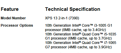
At Computex, Intel showed off a number of systems it says will be the leading designs for Ice Lake in Q4. These included a very impressive Dell XPS 13 system, a HP design with a wooden finish, and an Acer Swift model aiming to be the lightest Ice Lake laptop to come to market.
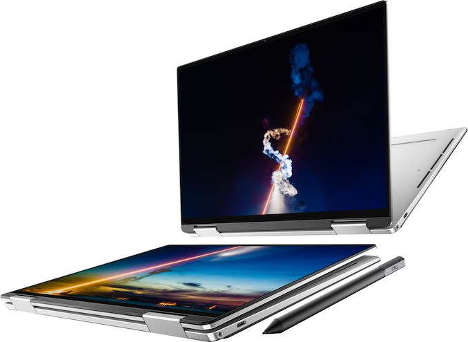
The Dell XPS 13
All of these devices come under Intel’s new Project Athena initiative.
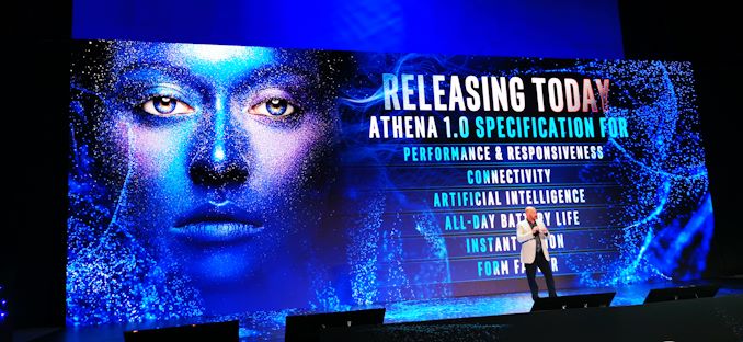
Project Athena borrows inspiration from Intel’s previous initiatives, such as Centrino and the Ultrabook. The goal here is to promote an ecosystem of Intel’s partners to design the next wave of devices and form factors that spurs on a good deal of innovation. This means that Project Athena has some very strict design targets that Intel’s partners have to follow and achieve in order to get the Athena designation/certification.

This means a lot of the following:
- Modern Connected Standby
- Biometric Login
- Wake from Sleep in <1 sec
- Core i5 or better
- >8GB DRAM in dual channel
- >256GB NVMe SSD, or Optane
- OpenVINO and WinML support
- 16+ hours of video playback
- 9+ hours of wireless web browsing
- Charge 4+hrs in 30 mins
- Thunderbolt 3, Wi-Fi 6, Gigabit LTE (optional)
- 2-in-1 or Clamshell,
- 12-15.6 inch, minimum resolution 1080p, touch display, narrow bezel on 3 sides
- Backlit keyboard, precision touchpad, pen support
Truth be told, supporting all of these means that the laptop should be a good buy with a decent user experience. These are a great set of goals to have for a mobile device, and it looks set that devices with the Athena designation should be very good.
However something to keep in mind is that in order to enable some of these technologies, it requires the OEMs to invest into Intel’s component ecosystem. Battery life, for example, helps if OEMs use the sub-1W panels that Intel has designated suitable for these devices. To implement Thunderbolt 3 and Wi-Fi 6 in a system is easy if a vendor uses an Ice Lake CPU, which also means that OEMs have to buy Intel’s AX200 chips (or a Killer AX1650, which is an AX200 underneath) to get Wi-Fi 6 to work. For Thunderbolt 3, re-timers are needed to support Type-C, and Intel makes those. The only other way to implement these features requires add-in cards which are higher power, and using those makes hitting the battery life targets, or the form factor requirements, difficult. Ultimately, to get the best of the Project Athena targets, the only way to do so is to buy more components from Intel or Intel approved component suppliers. Some may argue that programs like Project Athena end up cutting competition in this regard.
It should be noted that Ice Lake isn’t a requirement for Athena. But at this point it really, really, helps.
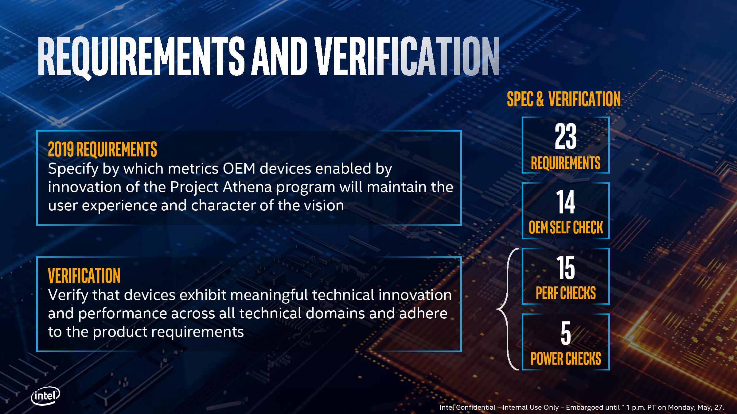
Intel will give the final Athena certification with a verification platform. This certification is built around what Intel says are ‘Key Experience Indicators’, such as the device being ready-to-go at a moment’s notice, providing enough worry-free battery life for common office tasks, and maintaining consistent responsiveness regardless of the state of the system.
Expect to see Athena devices in the market in Q4.
This Article
In this article, we’ll be going over Intel’s disclosures on Ice Lake, its new core Sunny Cove, as well as the new supported features and technologies within. We also comment on each of the new implemented items, with respect to user experience and realistic market/industry responses.


107 Comments
View All Comments
repoman27 - Tuesday, July 30, 2019 - link
"It stands to reason then that the smaller package is for lower performance and low power options, despite being exactly the same silicon."I know the die floorplans are the same, but have Intel ever actually confirmed that U and Y (or H and S series for that matter) are the exact same silicon? Is it strictly binning and packaging that separates the platforms, or is there a slight tweak to the manufacturing process to target lower power / higher frequencies? Intel production roadmaps would seem to indicate this isn't just a binning situation, but I've never been entirely certain on that point.
And isn't Comet Lake-U 6+2 more likely to be 25 W, with Whiskey Lake-U 4+2 continuing to pull 15 W duty alongside Ice Lake-U 4+2?
CaedenV - Tuesday, July 30, 2019 - link
Those goals for Aethena are OK, but my old Dell XPS 12 with a carousel frame hit all of those except biometric, and wake from sleep in <1 sec... well, and the bezel... but that was due to the carousel design which I would LOVE to come back in a more modern form.Not saying these goals are bad... but if a 6 year old midrange laptop can hit almost all of them, then this isn't exactly aiming for something amazing.
AshlayW - Tuesday, July 30, 2019 - link
Quad core for 179 USD? What is this, 2015? No thanks.HStewart - Tuesday, July 30, 2019 - link
You do realize these are ultra-portable low power cpu's and not desktop chipsSamus - Tuesday, July 30, 2019 - link
Intel is a mess right now, the execution of this along with the naming scheme is ridiculous.shabby - Tuesday, July 30, 2019 - link
18% ipc gain and 20% clock lossPlace your bets how intel will spin this.
CHADBOGA - Tuesday, July 30, 2019 - link
I'm quite disappointed the issue of security mitigation in hardware was not addressed. o_OCityBlue - Saturday, August 3, 2019 - link
Disappointed, but not surprised.Security (and by inference the performance overhead required to implement proper security) is not important according to Anandtech/Ian Cutress. Which is obvious nonsense, so the only logical conclusion is that Anandtech are now a thoroughly biased outfit incapable of any critical reporting, which is quite sad particularly as it means all their articles (particularly when they relate to Intel) have to be read with a very heavy dose of cynicism.
eek2121 - Wednesday, July 31, 2019 - link
That picture of you biting a wafer is priceless.Santoval - Wednesday, July 31, 2019 - link
If Ice Lake-U has a ~3.5% higher single core performance (and, assuming the "multi-core overhead" is the same, multi-core performance as well) than Whiskey Lake-U despite having a 20% lower single core boost clock, then Sunny Cove must be an extremely impressive μarch. Or, er, that might not actually be the case : Ice Lake-U has a 18% higher IPC than the *original* Skylake of 2015, not Whiskey Lake. While Whiskey Lake is basically the same design it must have a somewhat higher IPC due to its much more mature process node and other optimizations.Let's be conservative and assume that Ice Lake-U (more specifically Sunny Cove) has a nice round 15% higher IPC than Whiskey Lake-U, with both at 15W. In that case, at a 20% lower boost clock Ice Lake-U should have a 5% lower performance than Whiskey Lake-U. Where is that +3.5% performance derived from then?
Even if we assumed that Ice Lake-U 18% IPC edge is over Whiskey Lake-U (highly unlikely, otherwise Intel would not have dug out the original Skylake from its computing grave) that would still translate to Ice Lake-U having a 1.5% lower single core performance than Whiskey Lake-U, rather than being 3.5% faster than it.
Maybe, just maybe, this is why Intel used just a single synthetic benchmark (surely compiled with aggressive flags and optimized for Intel CPUs) for that graph and avoided to disclose other synthetic benchmarks and real world use benchmarks? Is this also why they avoided to talk about CPU performance of Ice Lake in their Computex presentation, and instead focused on iGPU, Wifi and AI performance?
Based on the disclosed clocks and the "disclosed" (in obfuscated form) IPC of Ice Lake-U I just cannot see it being in any way faster than Whiskey Lake-U. It will probably also have worse power efficiency, since it has the same or higher TDP range at a much lower clock.