GlobalFoundries Unveils 12LP+ Technology: Massive Performance & Power Improvements
by Anton Shilov on September 25, 2019 12:00 PM EST- Posted in
- GlobalFoundries
- Semiconductors
- 14LPP
- 12nm
- 12LP
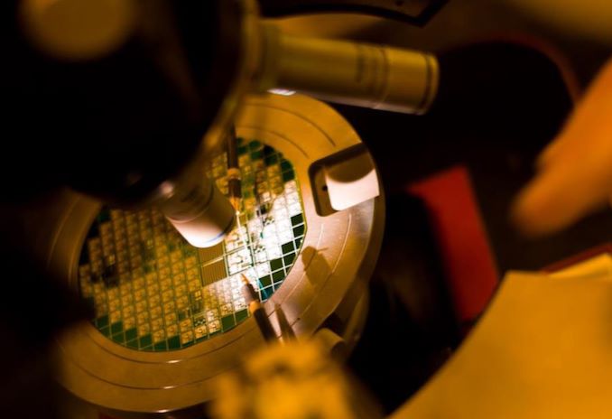
GlobalFoundries has introduced its 12LP+ fabrication process that relies on the groundwork set by its 14LPP and 12LP technologies and provides significant improvements when it comes to performance, power, and area (PPA) scaling. The specialty foundry positions the technology for developers of chips for cloud and edge AI applications.
GlobalFoundries’ 12LP+ manufacturing technology builds upon the company’s 12LP process yet enables a 20% increase in performance (at the same power and complexity) or a 40% reduction in power requirements (at the same clocks and complexity) as well as a 15% improvement in logic area scaling when compared to 12LP platform. Among other things, 12LP+ supports 0.5V SRAM bit cells (which probably use IP that the company designed for its 7 nm nodes). In addition, GF developed a new 2.5D interposer that enables 12LP+ SoCs to work with HBM memory.
| Advertised PPA Improvements of New Process Technologies Data announced by companies during conference calls, press briefings and in press releases |
||||||
| GlobalFoundries | ||||||
| 12LP+ vs 12LPP |
12LP vs 14LPP |
14HP vs 14LPP |
GF's 7nm Gen 1 vs 14LPP |
|||
| Power | 40% | - | ? | >60% | ||
| Performance | 20% | 10% | ? | >40% | ||
| Area Reduction | 15% | 15% | ? | >50% | ||
The foundry says that its 12LP+ uses a mature design and production ecosystem and provides advantages comparable to those of 7 nm-class fabrication process. Meanwhile, significant improvements and a new PDK point to new design libraries along with numerous new features, which means that GlobalFoundries’ clients will have to make significant investments in order to take advantage of 12LP+. Those investments will still be 50% lower than the cost of transition to a 7 nm-class technology, according to GlobalFoundries.
Michael Mendicino, vice president of Digital Technology Solutions at GF, said the following:
“Our 12LP+ solution already offers clients a majority of the performance and power advantages they would expect to gain from a 7nm process, but their NRE (non-recurring engineering) costs will average only about half as much, a significant savings. Additionally, because the 12 nm node has been running longer and is much more mature, clients will be able to tape-out quickly and take advantage of the growing demand for AI technology.”
To speed up development of 12LP+ chips for its clients, GlobalFoundries has asked Arm to design Arm Artisan physical IP and POP IP required by AI-focused SoCs. That IP is said to be compatible with 12LP. Meanwhile, the 12LP+ PDK is already available and several clients have begun to design chips using the technology. GlobalFoundries expects its customers to tape out the first 12LP+ SoCs sometimes in the second half of 2020 and produce them in volume in 2021.
GlobalFoundries will manufacture 12LP+ chips using deep ultraviolet (DUV) lithography with argon fluoride (ArF) excimer lasers operating on a 193 nm wavelength at its Fab 8 in New York, USA. Presumably, the company will use the same equipment that is currently used to make SoCs at 12LP and 14LPP nodes.
Related Reading:
- GlobalFoundries Adds 12LP Process for Mainstream and Automotive Chips; AMD Planning 12LP CPUs & GPUs
- GlobalFoundries Weds FinFET and SOI in 14HP Process Tech for IBM z14 CPUs
- GlobalFoundries Stops All 7nm Development: Opts To Focus on Specialized Processes
- Change of Strategy: A New GlobalFoundries CEO in Dr. Thomas Caulfield
- Samsung Details 11LPP Process Technology: 10 nm BEOL Meets 14 nm Elements
Source: GlobalFoundries


41 Comments
View All Comments
Tams80 - Thursday, September 26, 2019 - link
TSMC (and other leading fabs) are going to have to spend ever-increasing amounts on new nodes. Sure, they'll want to improve existing ones to remain profitable and help fund development, but a lot of their funds are going to be going into making transistors even smaller, etc.So, there's definitely a market there for older, bigger nodes. How long that market will last is questionable if a wall is hit at the frontier, but by then smaller fabs might have access to smaller nodes.
Kamen Rider Blade - Wednesday, September 25, 2019 - link
If older consoles ever decided to remanufacture their actual silicon, the power savings compared to the last node they were on would be immense. That would be great for one last hurrah on power savings and getting a new manufacture of an older console for gaming preservation.Tilmitt - Wednesday, September 25, 2019 - link
Would be cool to see this. Cell was shrunk twice from 90 nm to 65 then 45. I believe there were plans to bring it down to shrink it to 32nm that weren't followed through with. Imagine the yields and power efficiency you'd get with it on this process.Kamen Rider Blade - Thursday, September 26, 2019 - link
PS2's CPU/GPU ended on 65nm, imagine what you can do for that =DTechie2 - Wednesday, September 25, 2019 - link
It's always good for AMD to have multiple chip sources to cover their bases and negotiate the best prices. GloFo has served AMD well in the past and is likely to continue.Yojimbo - Wednesday, September 25, 2019 - link
Why are there so many comments about server CPUs and GPUs? Isn't this a low power process? They aren't going to be putting Epyc on a low power process. And volume production is expected in 2021. By that time cutting edge low power chips will be on the 5 nm node, not the 7 nm node. This seems like a lower cost alternative for non-high-end SOCs. So your lower and midrange smartphone SOCs might be built on this process. It also sounds like they are hoping for AI accelerators to use it, since they are mentioning compatibility with HBM, but that's probably more of a wish than something they are actually counting on.levizx - Sunday, September 29, 2019 - link
You do realise Epyc has an I/O die, right?Foeketijn - Thursday, September 26, 2019 - link
If I were AMD, I would ask GloFo to update the Epyc 3000 socs. (and rename them Opteron).That should go in the microserver gen11 and the like.
Now only supermicro really supplies Epyc soc boards. And that is a shame.
I like low powered highly dependable servers, and dislike the 2000's performance of an atom.
I bought a load of xeon E3's but am very willing to give AMD a try.
Kamen Rider Blade - Thursday, September 26, 2019 - link
Don't forget that AMD still has their Chipset & Central IO Die that they need to produce.The X570 could definitely use a node shrink along with the Central IO Die.
Don't forget the upcoming TRX40/80 & WRX80 chipsets.
All those could benefit from this process.
JoeDuarte - Monday, February 22, 2021 - link
I think there's a typo in the first data column of the comparison table. It compares 12LP+ to "12LPP".I don't think a node called 12LPP exists, certainly not from GlobalFoundries. It should be 12LP. That column means to compare the new node (12LP+) to its predecessor (12LP).