TSMC To Build 5nm Fab In Arizona, Set To Come Online In 2024
by Ryan Smith on May 15, 2020 10:00 AM EST- Posted in
- Semiconductors
- TSMC
- 5nm
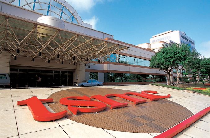
In a big shift to their manufacturing operations – and a big political win domestically – TSMC has announced that the company will be building a new, high-end fab in Arizona. The facility, set to come online in 2024, will utilize TSMC’s soon-to-be-deployed 5nm process, with the ability to handle 20,000 wafers a month. And with a final price tag on the facility expected to be $12 billion, this would make it one of the most expensive fabs ever built in the United States.
Operating over a dozen fabs across the globe, TSMC is responsible for a significant share of global logic chip production, particularly with leading-edge and near-leading-edge processes. The company has become perhaps the biggest winner amidst the gradual winnowing of fabs over the past two decades, as manufacturer after manufacturer has dropped out, consolidating orders among the remaining fabs. And with GlobalFoundries dropping out of the race for cutting-edge manufacturing nodes, TSMC is one of only three companies globally that's developing leading-edge process nodes – and one of the only two that’s a pure-play foundry.
This success has become both a boon and a liability for TSMC. Along with Korean rival Samsung, the two companies have seen massive growth in revenues and profits as they have become the last fabs standing. As a result, TSMC serves customers both locally and globally, particularly the United States and China, the two of which are not enjoying the best of relations right now. This leaves TSMC trapped in the middle of matters – both figuratively and literally – as China needs TSMC to produce leading-edge chips, and the United States is now increasingly reliant on TSMC as well following GlobalFoundries’ retreat.
As a result, the Taiwan Semiconductor Manufacturing Company is going to do something it’s never done before, building a near-leading-edge fab in the US, outside of its home base of Taiwan. The new facility, set to be constructed in Arizona, will use the company’s 5nm process, which is currently TSMC’s most advanced manufacturing process. And while this will no longer be the case by the time it comes online in 2024, when 3nm processes are likely to be available, it would still make the Arizona facility among the most advanced fabs in the world, and by far the most advanced contract fab in the United States.
The Arizona facility would be joining TSMC’s other US fab, which is located in Camas, Washington. It, like TSMC’s other non-Taiwanese-fabs, is based around older technologies, with the Camas fab in particular focusing on building flash products using relatively large process nodes (350nm to 160nm). As a result, the Arizona fab represents a significant shift for TSMC; it’s not the first US fab for the company, but it’s the first time TSMC has built such an advanced fab in another nation.
All told, the Arizona fab is set to be a medium-sized facility – a “megafab” in TSMC parlance – despite its use of an advanced manufacturing node. The 20,000 wafers per month throughput of the fab is well below TSMC’s largest “gigafabs” in Taiwan, which can move more than 100,000 wafers per month. As a result while the fab will add to TSMC’s 5nm capacity, it won’t become a massive part of that capacity. Though with an expected price tag of $12 billion, it will still be a very expensive facility to build.

According to TSMC, the primary impetus for building the fab – and especially to build it in the United States instead of Taiwan – is specifically to have high-end production capacity within the United States. With GlobalFoundries dropping out of the race for leading-edge nodes, the US government and other sensitive fabless chip designers are in want of another leading-edge facility within the US to build their chips. Given their location, TSMC’s Taiwanese fabs are seen as security risk, and the US would prefer to be self-reliant rather than relying on a foreign partner – a concern that’s been magnified by the current coronavirus pandemic and the supply chain issues that has created.
The end result is that while the fab is not explicitly reserved for military and other sensitive chips, it’s hard to imagine a scenario where the big commodity chip manufacturers such as AMD and Qualcomm don’t continue to use TSMC’s larger and more efficient fabs in Taiwan. In other words, while the Zen processor you’re playing World of Tanks on isn’t likely to come from Arizona, the chip that goes into an actual tank just might. Unaspiringly then, the planned Arizona fab comes with a lot of interest and support from both Arizona and the US Government, for both strategic and business reasons.
Interestingly, while the desire for more domestic fabs within the US has been well known, the US’s two major domestic fabs find themselves on the outside looking in with this deal. Intel has long tried to lure customers to its own contract manufacturing business, including making pitches to the US government, with little luck. Meanwhile GlobalFoundries is currently the US government’s preferred fab for military hardware – inheriting those fabs and the resulting business from IBM – but whom faces the prospect of slowly losing business as government customers switch to newer manufacturing processes. So in some respects it’s a bit surprising to see outsider TSMC land such a deal, though there are sizable political concerns involved as well.
At any rate, TSMC’s Arizona fab is expected to break ground in 2021, with completion scheduled for 2024. At which point it is anticipated to employ over 1600 workers as TSMC becomes the United States’ second leading-edge foundry provider.
Source: TSMC


97 Comments
View All Comments
brucethemoose - Friday, May 15, 2020 - link
"And while this will no longer be the case by the time it comes online in 2024, when 3nm processes are likely to be available"On schedule 7nm was a miracle, even for TSMC. I'll eat my shoe if 3nm comes on time.
Also, the projected tape out costs for 3nm are... eye opening. I think many products (or parts of products) are going to stay on 5nm, especially if physics start getting in the way of improvements other than density.
TimSyd - Saturday, May 16, 2020 - link
5nm is already online. 3nm is well underway but involves a completely new transistor so still likely to be tricky getting to production levels.Still by 2024 it would be surprising if 3nm is *not* available, most likely it would be a year or two old at that point and the 3nm refresh, 3nm+ node would be coming online.
nandnandnand - Saturday, May 16, 2020 - link
3nm was already delayed by 6 months due to coronavirus interference.https://www.tomshardware.com/news/samsung-3nm-rele...
Even with that delay, they expect volume production in 2022. So the article is almost certainly correct about 3nm being available in 2024.
Keep in mind that you have to evaluate the transistor density and other factors. "3nm" means nothing, they can call anything they want 3nm, just like other fabs have done with other nodes.
Wilco1 - Sunday, May 17, 2020 - link
That's Samsung's 3nm process, but TSMC recently said 3nm remains on schedule: https://fuse.wikichip.org/news/3453/tsmc-ramps-5nm...The nm numbers are just names, they haven't had any meaning for more than a decade. This is a good article comparing the next generation processes: https://semiwiki.com/semiconductor-manufacturers/i...
nandnandnand - Sunday, May 17, 2020 - link
I linked the wrong one:https://wccftech.com/tsmc-delays-the-production-of...
"TSMC Delays The Production Of 3nm By 6 Months Amidst Equipment Shortages In The Wake Of The Pandemic – 5nm Is Still On Schedule With Production At Full Capacity"
Whatever the case, they should be pumping out 3nm before the 5nm Arizona fab opens.
Cullinaire - Friday, May 15, 2020 - link
Looks like Intel is going to see big competition for good fab workers finally. A lot of poaching is going to happen, what a headache for Intel.yeeeeman - Saturday, May 16, 2020 - link
Bad decision, but I guess being pressured by US govnment is not an easy task.nandnandnand - Saturday, May 16, 2020 - link
How are you qualified to call it a "bad decision"?MASSAMKULABOX - Saturday, May 16, 2020 - link
Thee is a graph showing the increasing cost of Fabs as the Nodes go smaller . 1 nm will likley cost over a Trillion dollars per fab (jk).Shouldnt we be getting huge cheap reliable SSD's, Flash drives and emmc from all this. back to the 70's for the FAB workers, groovy Babe...
nandnandnand - Saturday, May 16, 2020 - link
I was 'bout to scoff at the 1 trillion comment.It doesn't matter. 2-5 fabs (TSMC, Samsung, Intel...) will get down to whatever they want to call "1nm" (these are marketing names). Then other fabs will start creating monolithic 3D CPUs that can beat even "1nm" from older process nodes like "32nm". Then monolithic 3D designs will be shrunk down to use "5nm" or lower and you'll have absurdly powerful and dense chips. Maybe that will be the end of Moore's law, maybe not.