AMD Zen 3 Ryzen Deep Dive Review: 5950X, 5900X, 5800X and 5600X Tested
by Dr. Ian Cutress on November 5, 2020 9:01 AM EST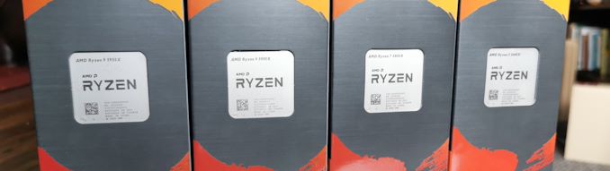
When AMD announced that its new Zen 3 core was a ground-up redesign and offered complete performance leadership, we had to ask them to confirm if that’s exactly what they said. Despite being less than 10% the size of Intel, and very close to folding as a company in 2015, the bets that AMD made in that timeframe with its next generation Zen microarchitecture and Ryzen designs are now coming to fruition. Zen 3 and the new Ryzen 5000 processors, for the desktop market, are the realization of those goals: not only performance per watt and performance per dollar leaders, but absolute performance leadership in every segment. We’ve gone into the new microarchitecture and tested the new processors. AMD is the new king, and we have the data to show it.
New Core, Same 7nm, Over 5.0 GHz!
The new Ryzen 5000 processors are drop-in replacements for the Ryzen 3000 series. Anyone with an AMD X570 or B550 motherboard today, with the latest BIOS (AGESA 1081 or above), should be able to buy and use one of the new processors without a fuss. Anyone with an X470/B450 board will have to wait until Q1 2021 as those boards are updated.
As we’ve previously covered, AMD is launching four processors today for retail, ranging from six cores up to sixteen cores.
| AMD Ryzen 5000 Series Processors Zen 3 Microarchitecture |
||||||
| AnandTech | Cores Threads |
Base Freq |
Turbo Freq |
L3 Cache |
TDP | MSRP |
| Ryzen 9 5950X | 16c/32t | 3400 | 4900 | 64 MB | 105 W | $799 |
| Ryzen 9 5900X | 12c/24t | 3700 | 4800 | 64 MB | 105 W | $549 |
| Ryzen 7 5800X | 8c/16t | 3800 | 4700 | 32 MB | 105 W | $449 |
| Ryzen 5 5600X | 6c/12t | 3700 | 4600 | 32 MB | 65 W | $299* |
*Comes with Bundled CPU Cooler
All the processors have native support for DDR4-3200 memory as per JEDEC standards, although AMD recommends something slightly faster for optimum performance. All the processors also have 20 lanes of PCIe 4.0 for add-in devices.
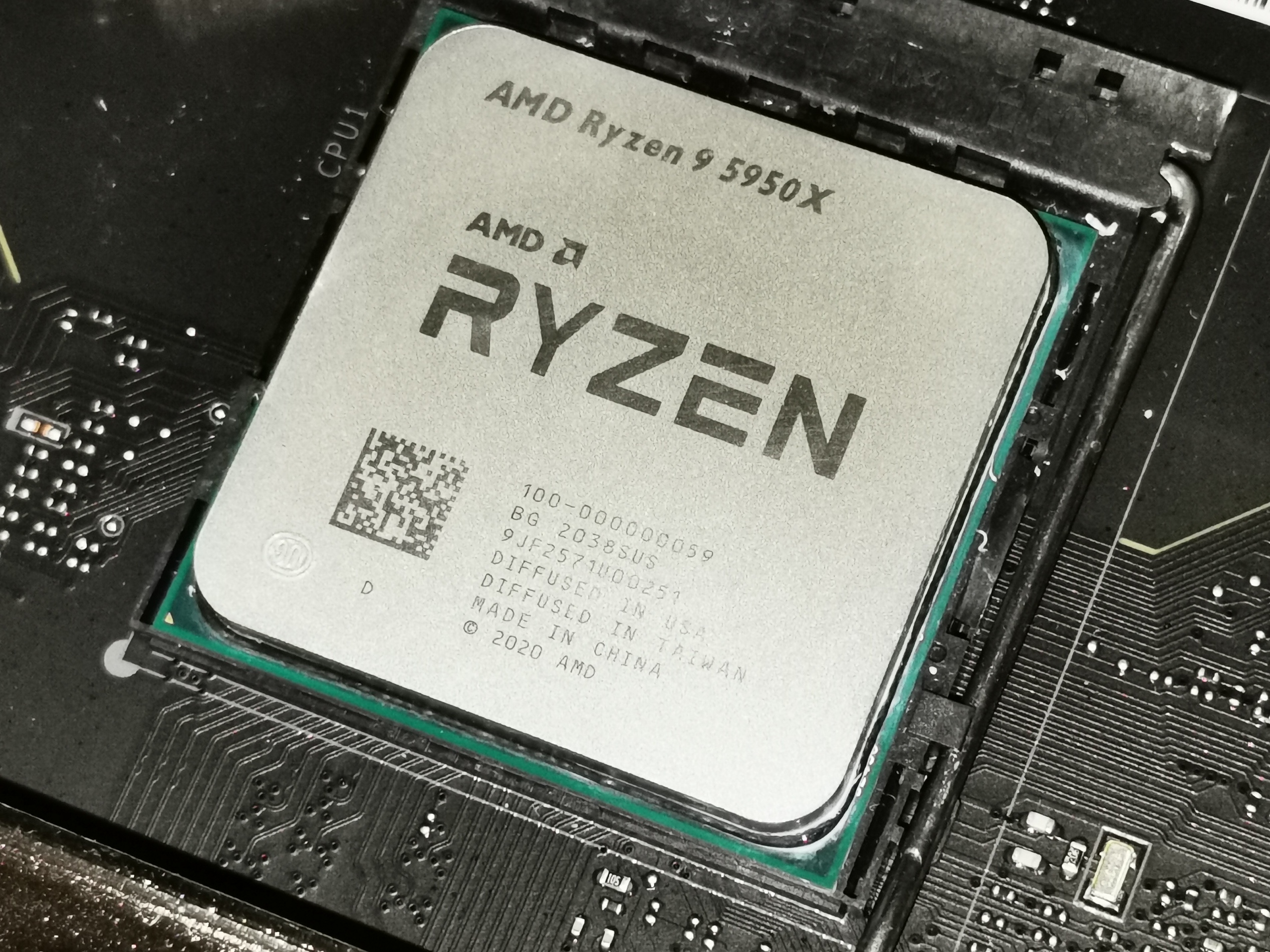
The Ryzen 9 5950X: 16 Cores at $799
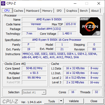
The top processor is the Ryzen 9 5950X, with 16 cores and 32 threads, offering a base frequency of 3400 MHz and a turbo frequency of 4900 MHz – on our retail processor, we actually detected a single core frequency of 5050 MHz, indicating that this processor will turbo above 5.0 GHz with sufficient thermal headroom and cooling!
This processor is enabled through two eight core chiplets (more on chiplets below), each with 32 MB of L3 cache (total 64 MB). The Ryzen 9 5950X is rated at the same TDP as the Ryzen 9 3950X, at 105 W. The peak power will be ~142 W, as per AMD’s socket design, on motherboards that can support it.
For those that don’t read the rest of the review, the short conclusion for the Ryzen 9 5950X is that even at $799 suggested retail price, it enables a new level of consumer grade performance across the board. The single thread frequency is crazy high, and when combined with the new core design with its higher IPC, pushes workloads that are single-core limited above and beyond Intel’s best Tiger Lake processors. When it comes to multi-threaded workloads, we have new records for a consumer processor across the board.
The Ryzen 9 5900X: 12 Cores at $549
Squaring off against Intel’s best consumer grade processor is the Ryzen 9 5900X, with 12 cores and 24 threads, offering a base frequency of 3700 MHz and a turbo frequency of 4800 MHz (4950 MHz was observed). This processor is enabled through two six-core chiplets, but all the cache is still enabled at 32 MB per chiplet (64 MB total). The 5900X also has the same TDP as the 3900X/3900XT it replaces at 105 W.
At $549, it is priced $50 higher than the processor it replaces, which means that for the extra 10% cost it will have to showcase that it can perform at least 10% better.
The Ryzen 7 5800X: 8 Cores at $449
After AMD showcased a quad core processor under $100 in the last generation, it takes a lot of chutzpah to offer an eight core processor for $449 – AMD stands by its claims that this processor offers substantial generational performance improvements. The new AMD Ryzen 7 5800X, with eight cores and sixteen threads, is set to go up against Intel’s Core i7-10700K, also an eight core / sixteen thread processor.
The Ryzen 7 5800X has a base frequency of 3800 MHz and a rated turbo frequency of 4700 MHz (we detected 4825 MHz), and uses a single eight-core chiplet with a total 32 MB of L3 cache. The single core chiplet has some small benefits over a dual chiplet design where some cross-CPU communication is needed, and that comes across in some of our very CPU-limited gaming benchmarks. This processor also has 105 W TDP (~142 W peak).
The Ryzen 5 5600X: 6 Cores for $299
The cheapest processor that AMD is releasing today is the Ryzen 5 5600X, but it is also the only one that comes with a CPU cooler in box. The Ryzen 5 5600X has six cores and twelve threads, running at a base frequency of 3700 MHz and a peak turbo of 4600 MHz (4650 MHz measured), and is the only CPU to be given a TDP of 65 W (~88 W peak).
The single chiplet design means 32 MB of L3 cache total (technically it’s still the same that a single core can access as the Ryzen 9 parts, more on that later), and will be put up against Intel’s six-core Core i5-10600K, which also retails in a similar ballpark.
Despite being the cheapest and technically the slowest processor of the bunch, I was mightily surprised by the performance of the Ryzen 5 5600X: similar to the Ryzen 9 5950X, in single threaded benchmarks, it completely knocks the socks off of anything Intel has to offer – even Tiger Lake.
Why Ryzen 5000 Works: Chiplets
At a high level, the new Ryzen 5000 'Vermeer' series seem oddly familiar to the last generation Ryzen 3000 ‘Matisse’ series. This is actually by design, as AMD is fully leveraging their chiplet design methodology in the new processors.
To introduce some terminology, AMD creates two types of chiplets. One of them has the main processing cores, and is called a core complex die or CCD. This is the one that is built on TSMC's 7nm process. The other chiplet is an interconnect die with I/O, known as an IO die or IOD - this one has the PCIe lanes, the memory controllers, the SATA ports, the connection to the chipset, and helps control power delivery as well as security. In both the previous generation and the new generation, AMD pairs one of its IO dies with up to two 8-core chiplets.
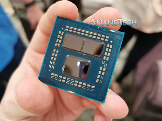
Ryzen 3000 processor without heatspreader, showing two core chiplets and one IO die.
This is possible because the new core chiplets contain the same protocols for interconnect, physical design, and power constraints. AMD is able to leverage the execution of the previous platform and generation such that when the core connections are identical, despite the different internal structures (Zen 3 vs Zen 2), they can still be put together and executed in a known and successful fashion.
As with the previous generation, the new Zen 3 chiplet is designed with eight cores
Zen 3 is a New Core Design
By keeping the new 8-core Zen 3 chiplet the same size and same power, this obviously means that AMD had to build a core that fits within those constraints but also affords a performance and performance efficiency uplift in order to make a more compelling design. Typically when designing a CPU core, the easiest thing to do is to take the previous design and upgrade certain parts of it – or what engineers call tackling ‘the low hanging fruit’ which enables the most speed-up for the least effort. Because CPU core designs are built to a deadline, there are always ideas that never make it into the final design, but those become the easiest targets for the next generation. This is what we saw with Zen 1/Zen+ moving on to Zen 2. So naturally, the easiest thing for AMD to do would be the same again, but with Zen 3.
However, AMD did not do this. In our interviews with AMD’s senior staff, we have known that AMD has two independent CPU core design teams that aim to leapfrog each other as they build newer, high performance cores. Zen 1 and Zen 2 were products from the first core design team, and now Zen 3 is the product from the second design team. Naturally we then expect Zen 4 to be the next generation of Zen 3, with ‘the low hanging fruit’ taken care of.
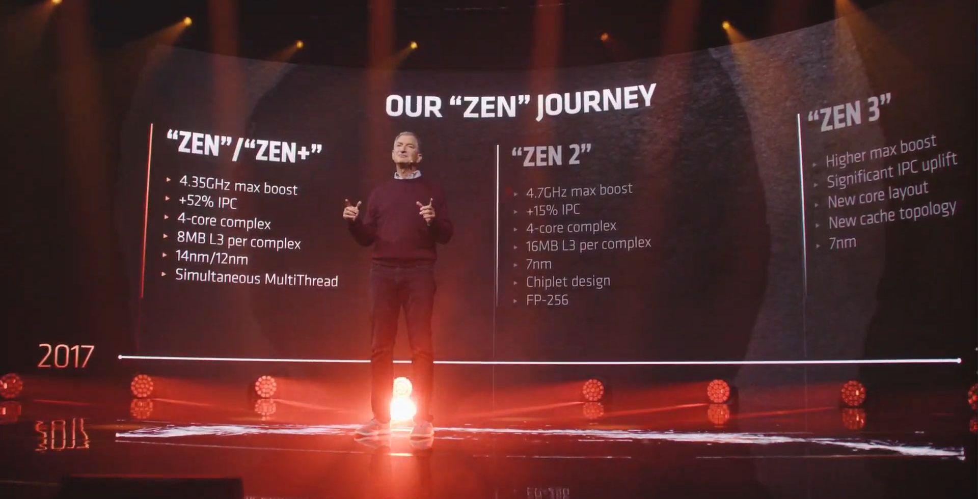
In our recent interview with AMD’s Chief Technology Officer, Mark Papermaster, we were told that if you were to look at the core from a 100,000 foot level, you might easily mistake that the Zen 3 core design to be similar to that of Zen 2. However, we were told that because this is a new team, every segment of the core has been redesigned, or at the very least, updated. Users who follow this space closely will remember that the branch predictor used in Zen 2 wasn’t meant to come until Zen 3, showing that even the core designs have an element of portability to them. The fact that both Zen 2 and Zen 3 are built on the same TSMC N7 process node (the same PDK, although Zen 3 has the latest yield/consistency manufacturing updates from TMSC) also helps in that design portability.
AMD has already announced the major change that will be obvious to most of the techies that are interested in this space: the base core chiplet, rather than having two four-core complexes, has a single eight-core complex. This enables each core to access the whole 32 MB of L3 cache of a die, rather than 16 MB, which reduces latency of memory accesses in that 16-to-32 MB window. It also simplifies core-to-core communication within a chiplet. There are a couple of trade-offs to do this, but overall it is a good win.
In fact there are a significant number of differences throughout the core. AMD has improved:
- branch prediction bandwidth
- faster switching from the decode pipes to the micro-op cache,
- faster recoveries from mispredicts,
- enhanced decode skip detection for some NOPs/zeroing idioms
- larger buffers and execution windows up and down the core,
- dedicated branch pipes,
- better balancing of logic and address generation,
- wider INT/FP dispatch,
- higher load bandwidth,
- higher store bandwidth,
- better flexibility in load/store ops
- faster FMACs
- A wide variety of faster operations (including x87?)
- more TLB table walkers
- better prediction of store-to-load forward dependencies
- faster copy of short strings
- more AVX2 support (VAES, VPCLMULQD)
- substantially faster DIV/IDIV support
- hardware acceleration of PDEP/PEXT
Many of these will be explained and expanded upon over the next few pages, and observed in the benchmark results. Simply put, this is something more than just a core update – these are genuinely new cores and new designs that required new sheets of paper to be built upon.
A number of these features, such as wider buffers and increased bandwidth, naturally come with the question about how AMD has kept the power the same for Zen 3 compared to Zen 2. Normally when a core gets wider, that means more silicon has to be turned on all the time, and this influences static power, or if it all gets used simultaneously, then there is higher active power.
When speaking with Mark Papermaster, he pointed to AMD’s prowess in physical implementation as a key factor in this. By leveraging their knowledge of TSMC’s 7nm (N7) process, as well as updates to their own tools to get the best out of these designs, AMD was able to remain power neutral, despite all this updates and upgrades. Part of this also comes from AMD’s long standing premium partner relationship with TMSC, being able to enable better design technology co-optimization (DTCO) between floorplan, manufacturing, and product.
AMD’s Claims
The CPU marketing teams from AMD, since the launch of first generation Zen, have been very accurate in their performance claims, even to the point of understating performance from time to time. Aside from promoting performance leadership in single thread, multi-thread, and gaming, AMD promoted several metrics for generation-on-generation improvement.
+19% IPC
The key metric offered by AMD was a +19% IPC uplift from Zen 2 to Zen 3, or rather a +19% uplift from Ryzen 5 3800XT to Ryzen 5 5800X when both CPUs are at 4.0 GHz and using DDR4-3600 memory.
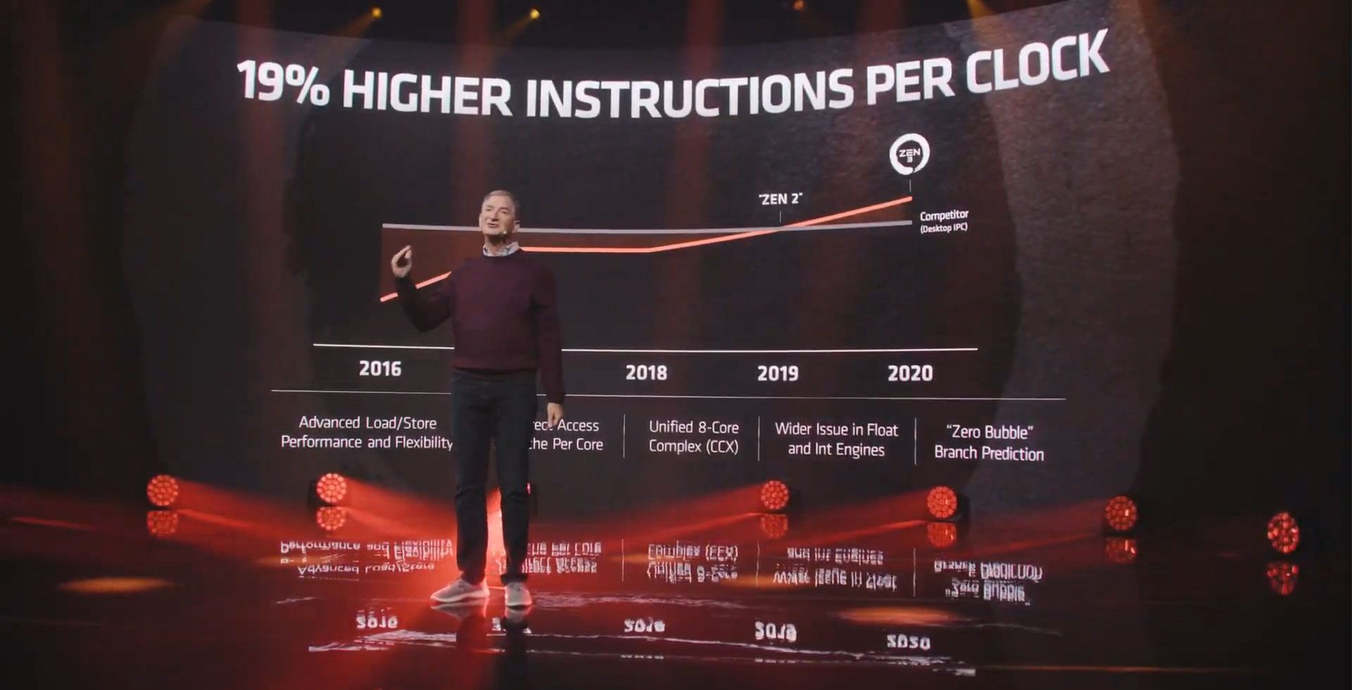
In fact, using our industry benchmarks, for single threaded performance, we observed a +19% increase in CPU performance per clock. We have to offer kudos to AMD here, this is the second or third time they've quoted IPC figures which we've matched.
In multithreaded SPECrate, the absolute gain was only around 10% or so, given that faster cores also require more bandwidth to main memory, which hasn’t been provided in this generation. This means that there are some bottlenecks to which a higher IPC won’t help if more cores require the same resources.
For real-world tests, across our whole suite, we saw an average +24% uplift. For explicitly multithreaded tests, we saw ranges from even performance up to +35%, while for explicitly single threaded tests, this ranged from even performance up to +57%. This comes down to execution/compute bound tests getting bigger speedups over memory bound workloads.
Best Gaming
For gaming, the number was given as a +5 to +50% uplift in 1920x1080 gaming at the high preset, comparing a Ryzen 9 5900X against the Ryzen 9 3900XT, depending on the benchmark.
In our tests at CPU limited settings, such as 720p or 480p minimum, we saw an average +44% frames-per-second performance uplift comparing the Ryzen 9 5950X to the Ryzen 9 3950X. Depending on the test, this ranged from +10% to +80% performance uplift, with key gains in Chernobylite, Borderlands 3, Gears Tactics, and F1 2019.
For our more mainstream gaming tests, run at 1920x1080 with all the quality settings on maximum, the performance gain averaged around +10%. This spanned the gamut from an equal score (World of Tanks, Strange Brigade, Red Dead Redemption), up to +36% (Civilization 6, Far Cry 5).
Perhaps the most important comparison is the AMD Ryzen 9 5950X against the Intel Core i9-10900K. In our CPU limited tests, we get a +21% average FPS win for the AMD at CPU-limited scenarios, ranging from +2% to +52%. But in our 1080p Maximum settings tests, the results were on average neck-and-neck, swaying from -4% to +6%. (That result doesn’t include the one anomaly in our tests, as Civilization 6 shows a +43% win for AMD.)
Head-to-Head Performance Matchups
Based on core counts and pricing, the new Ryzen 5000 series processors closely align with some of Intel’s most popular Comet Lake processors, as well as the previous generation AMD hardware.
| Q4 2020 Matchups | ||||||
| AMD Ryzen 5000 |
Cores | SEP | Tray 1ku |
Cores | Intel Core 10th Gen |
|
| Ryzen 9 5950X | 16C | $799 | vs. | $999 | 18C | Core i9-10980XE* |
| Ryzen 9 5900X | 12C | $549 | vs. | $488 | 10C | Core i9-10900K |
| Ryzen 7 5800X | 8C | $449 | vs. | $453 | 10C | Core i9-10850K |
| $374 | 8C | Core i7-10700K | ||||
| Ryzen 5 5600X | 6C | $299 | vs. | $262 | 6C | Core i5-10600K |
*Technically a high-end desktop platform processor, almost unavailable at MSRP.
Throughout this review we will be referencing these comparisons, and will eventually break-out each processor into its own analysis breakdown.
More In This Review
As this is our Deep Dive coverage into Zen 3, we are going to go into some nitty-gritty details. Over the next few pages, we will go over:
- Improvements to the core design (prefetchers, buffers, execution units, etc)
- Our microbenchmark tests (core-to-core latency, cache hierarchy, turbo ramping)
- New Instructions, Improved instructions
- SoC Power and Per-Core Power
- SPEC2006 and SPEC2017 results
- CPU Benchmarks (Office, Science, Simulation, Rendering, Encoding, Web, Legacy)
- Gaming Benchmarks (11 tests, 4 settings per test, with RTX 2080 Ti)
- Conclusions and Final Remarks


339 Comments
View All Comments
TheinsanegamerN - Tuesday, November 10, 2020 - link
However AMD's boost algorithim is very temperature sensitive. Those coolers may work fine, but if they get to the 70C range you're losing max performance to higher temperatures.Andrew LB - Sunday, December 13, 2020 - link
Blah blah....Ryzen 5800x @ 3.6-4.7ghz : 219w and 82'c.
Ryzen 5800x @ 4.7ghz locked: 231w and 88'c.
Fractal Celsius+ S28 Prisma 280mm AIO CPU cooler at full fan and pump speed
https://www.kitguru.net/components/cpu/luke-hill/a...
If you actually set your voltages on Intel chips they stay cool. My i7-10700k @ 5.0ghz all-core locked never goes above 70'c.
Count Rushmore - Friday, November 6, 2020 - link
It took 3 days... finally the article load-up.AT seriously need to upgrade their server (or I need to stop using IE6).
name99 - Friday, November 6, 2020 - link
"AMD wouldn’t exactly detail what this means but we suspect that this could allude to now two branch predictions per cycle instead of just one"So imagine you have wide OoO CPU. How do you design fetch? The current state of the art (and presumably AMD have aspects of this, though perhaps not the *entire* package) goes as follows:
Instructions come as runs of sequential instructions separated by branches. At a branch you may HAVE to fetch instructions from a new address (think call, goto, return) or you may perhaps continue to the next address (think non-taken branch).
So an intermediate complexity fetch engine will bring in blobs of instructions, up to (say 6 or 8) with the run of instructions terminating at
- I've scooped up N or
- I've hit a branch or
- I've hit the end of a cache line.
Basically every cycle should consist of pulling in the longest run of instructions possible subject to the above rules.
The way really advanced fetch works is totally decoupled from the rest of the CPU. Every cycle the fetch engine predicts the next fetch address (from some hierarchy of : check the link stack, check the BTB, increment the PC), and fetches as much as possible from that address. These are stuck in a queue connected to decode, and ideally that queue would never run dry.
BUT: on average there is about a branch every 6 instructions.
Now supposed you want to sustain, let's say, 8-wide. That means that you might set N at 8, but most of the time you'll fetch 6 or so instructions because you'll bail out based on hitting a branch before you have a full 8 instructions in your scoop. So you're mostly unable to go beyond an IPC of 6, even if *everything* else is ideal.
BUT most branches are conditional. And good enough half of those are not taken. This means that if you can generate TWO branch predictions per cycle then much of the time the first branch will not be taken, can be ignored, and fetch can continue in a straight line past it. Big win! Half the time you can pull in only 6 instructions, but the other half you could pull in maybe 12 instructions. Basically, if you want to sustain 8 wide, you'd probably want to pull in at least 10 or 12 instructions under best case conditions, to help fill up the queue for the cases where you pull in less than 8 instructions (first branch is taken, or you reach the end of the cache line).
Now there are some technicalities here.
One is "how does fetch know where the branches are, to know when to stop fetching". This is usually done via pre-decode bits living in the I-cache, and set by a kinda decode when the line is first pulled into the I-cache. (I think x86 also does this, but I have no idea how. It's obviously much easier for a sane ISA like ARM, POWER, even z.)
Second, and more interesting, is that you're actually performing two DIFFERENT TYPES of prediction, which makes it somewhat easier from a bandwidth point of view. The prediction on the first branch is purely "taken/not taken", and all you care about is "not taken"; the prediction on the second branch is more sophisticated because if you predict taken you also have to predict the target, which means dealing BTB or link stack.
But you don't have to predict TWO DIFFERENT "next fetch addresses" per cycle, which makes it somewhat easier.
Note also that any CPU that uses two level branch prediction is, I think, already doing two branch prediction per cycle, even if it doesn't look like it. Think about it: how do you USE a large (but slow) second level pool of branch prediction information?
You run the async fetch engine primarily from the first level; and this gives a constant stream of "runs of instructions, separated by branches" with zero delay cycles between runs. Great, zero cycle branches, we all want that. BUT for the predictors to generate a new result in a single cycle they can't be too large.
So you also run a separate engine, delayed a cycle or two, based on the larger pool of second level branch data, checking the predictions of the async engine. If there's a disagreement you flush whatever was fetched past that point (which hopefully is still just in the fetch queue...) and resteer. This will give you a one (or three or four) cycle bubble in the fetch stream, which is not ideal, but
- it doesn't happen that often
- it's a lot better catching a bad prediction very early in fetch, rather than much later in execution
- hopefully the fetch queue is full enough, and filled fast enough, that perhaps it's not even drained by the time decode has walked along it to the point at which the re-steer occurred...
This second (checking) branch prediction doesn't ever get mentioned, but it is there behind the scenes, even when the CPU is ostensibly doing only a single prediction per cycle.
There are other crazy things that happen in modern fetch engines (which are basically in themselves as complicated as a whole CPU from 20 years ago).
One interesting idea is to use the same data that is informing the async fetch engine to inform prefetch. The idea is that you now have essentially two fetch engines running. One is as I described above; the second ONLY cares about the stream of TAKEN branches, and follows that stream as rapidly as possible, ensuring that each line referenced by this stream is being pulled into the I-cache. (You will recognize this as something like a very specialized form of run-ahead.)
In principle this should be perfect -- the I prefetcher and branch-prediction are both trying to solve the *exact* same problem, so pooling their resources should be optimal! In practice, so far this hasn't yet been perfected; the best simulations using this idea are a very few percent behind the best simulations using a different I prefetch technology. But IMHO this is mostly a consequence of this being a fairly new idea that has so far been explored mainly by using pre-existing branch predictors, rather than designing a branch predictor store that's optimal for both tasks.
The main difference is that what matters for prefetching is "far future" branches, branches somewhat beyond where I am now, so that there's plenty of time to pull in the line all the way from RAM. And existing branch predictors have had no incentive to hold onto that sort of far future prediction state. HOWEVER
A second interesting idea is what IBM has been doing for two or three years now. They store branch prediction in what they call an L2 storage but, to avoid things, I'll cal a cold cache. This is stale/far future branch prediction data that is unused for a while but, on triggering events, that cold cache data will be swapped into the branch prediction storage so that the branch predictors are ready to go for the new context in which they find themselves.
I don't believe IBM use this to drive their I-prefetcher, but obviously it is a great solution to the problem I described above and I suspect this will be where all the performance CPUs eventually find themselves over the next few years. (Apple and IBM probably first, because Apple is Apple, and IBM has the hard part of the solution already in place; then ARM because they's smart and trying hard; then AMD because they're also smart but their technology cycles are slower than ARM; and final Intel because, well, they're Intel and have been running on fumes for a few years now.)
(Note of course this only solves I-prefetch, which is nice and important; but D-prefetch remains as a difficult and different problem.)
name99 - Friday, November 6, 2020 - link
Oh, one more thing. I referred to "width" of the CPU above. This becomes an ever vaguer term every year. The basic points are two:- when OoO started, it seemed reasonable to scale every step of the pipeline together. Make the CPU 4-wide. So it can fetch up to 4 instructions/cycle. decode up to 4, issue up to 4, retire up to 4. BUT if you do this you're losing performance every step of the way. Every cycle that fetches only 3 instructions can never make that up; likewise every cycle that only issues 3 instructions.
- so once you have enough transistors available for better designs, you need to ask yourself what's the RATE-LIMITING step? For x86 that's probably in fetch and decode, but let's consider sane ISAs like ARM. There the rate limiting step is probably register rename. So lets assume your max rename bandwidth is 6 instructions/cycle. You actually want to run the rest of your machinery at something like 7 or 8 wide because (by definition) you CAN do so (they are not rate limiting, so they can be grown). And by running them wider you can ensure that the inevitable hiccups along the way are mostly hidden by queues, and your rename machinery is running at full speed, 6-wide each and every cycle, rather than frequently running at 5 or 4 wide because of some unfortunate glitch upstream.
Spunjji - Monday, November 9, 2020 - link
These were interesting posts. Thank you!GeoffreyA - Monday, November 9, 2020 - link
Yes, excellent posts. Thanks.Touching on width, I was expecting Zen 3 to add another decoder and take it up to 5-wide decode (like Skylake onwards). Zen 3's keeping it at 4 makes good sense though, considering their constraint of not raising power. Another decoder might have raised IPC but would have likely picked up power quite a bit.
ignizkrizalid - Saturday, November 7, 2020 - link
Rip Intel no matter how hard you try squeezing Intel sometimes on top within your graphics! stupid site bias and unreliable if this site was to be truth why not do a live video comparison side by side using 3600 or 4000Mhz ram so we can see the actual numbers and be 100% assured the graphic table is not manipulated in any way, yea I know you will never do it! personally I don't trust these "reviews" that can be manipulated as desired, I respect live video comparison with nothing to hide to the public. Rip Intel Rip Intel.Spunjji - Monday, November 9, 2020 - link
I... don't think this makes an awful lots of sense, tbh.MDD1963 - Saturday, November 7, 2020 - link
It would be interesting to also see the various results of the 10900K the way most people actually run them on Z490 boards, i.e, with higher RAM clocks, MCE enabled, etc...; do the equivalent tuning with 5000 series, I'm sure they will run with faster than DDR4-3200 MHz. plus perhaps a small all-core overclock.