Intel’s Integrated Graphics Mini-Review: Is Rocket Lake Core 11th Gen Competitive?
by Dr. Ian Cutress on May 7, 2021 10:20 AM EST
In the last few months we have tested the latest x86 integrated graphics options on the desktop from AMD, with some surprising results about how performant a platform with integrated graphics can be. In this review, we’re doing a similar test but with Intel’s latest Rocket Lake Core 11th Gen processors. These processors feature Intel’s Xe-LP graphics, which were touted as ‘next-generation’ when they launched with Intel’s mobile-focused Tiger Lake platform. However, the version implemented on Rocket Lake has fewer graphics units, slower memory, but a nice healthy power budget to maximize. Lo, Intel set forth for battle.
When a CPU meets GPU
Intel initially started integrating graphics onto its systems in 1999, by pairing the chipset with some form of video output. In 2010, the company moved from chipset graphics to on-board processor graphics, enabling the graphics hardware to take advantage of a much faster bandwidth to main memory as well as a much lower latency. Intel’s consumer processors now feature integrated graphics as the default configuration, with Intel at times dedicating more of the processor design to graphics than to actual cores.
| Intel CPUs: IGP as a % of Die Area | ||||||
| AnandTech | Example | Launched | Cores | IGP | Size | IGP as Die Area % |
| Sandy Bridge | i7-2600K | Jan 2011 | 4 | Gen6 | GT2 | 11% |
| Ivy Bridge | i7-3770K | April 2012 | 4 | Gen7 | GT2 | 29% |
| Haswell | i7-4770K | June 2013 | 4 | Gen7.5 | GT2 | 29% |
| Broadwell | i7-5775C | June 2015 | 4 | Gen8 | GT3e | 48% |
| Skylake | i7-6700K | Aug 2015 | 4 | Gen9 | GT2 | 36% |
| Kaby Lake | i7-7700K | Jan 2017 | 4 | Gen9 | GT2 | 36% |
| Coffee Lake | i7-8700K | Sept 2017 | 6 | Gen9 | GT2 | 30% |
| Coffee Lake | i9-9900K | Oct 2018 | 8 | Gen9 | GT2 | 26% |
| Comet Lake | i9-10900K | April 2020 | 10 | Gen9 | 24 EUs | 22% |
| Rocket Lake | i9-11900K | March 2021 | 8 | Xe-LP | 32 EUs | 21% |
| Mobile CPUs | ||||||
| Ice Lake-U | i7-1065G7 | Aug 2019 | 4 | Gen11 | 64 EUs | 36% |
| Tiger Lake-U | i7-1185G7 | Sept 2020 | 4 | Xe-LP | 96 EUs | 32% |
All the way from Intel’s first integrated graphics to its 2020 product line, Intel was reliant on its ‘Gen’ design. We saw a number of iterations over the years, with updates to the function and processing ratios, with Gen11 featuring heavily in Intel’s first production 10nm processor, Ice Lake.
The latest graphics design however is different. No longer called ‘Gen’, Intel upcycled its design with additional compute, more features, and an extended effort for the design to scale from mobile compute all the way up to supercomputers. This new graphics family, known as Xe, is now the foundation of Intel’s graphics portfolio. It comes in four main flavors:
- Xe-HPC for High Performance Computing in Supercomputers
- Xe-HP for High Performance and Optimized FP64
- Xe-HPG for High Performance Gaming with Ray Tracing
- Xe-LP for Low Power for Integrated and Entry Level
Intel has initially rolled out its LP designs into the market place, first with its Tiger Lake mobile processors, then with its Xe MAX entry level notebook graphics card, and now with Rocket Lake.
Xe-LP, A Quick Refresher
Intel’s LP improves on the previous Gen11 graphics by reorganizing the base structure of the design. Rather than 7 logic units per execution unit, we now have 8, and LP’s front-end can dispatch up two triangles per clock rather than one. The default design of LP involves 96 execution units, split into a centralized ‘slice’ that has all the geometry features and fixed function hardware, and up to 6 ‘sub-slices’ each with 16 logic units and 64 KiB of L1 cache. Each variant of LP can then have up to 96 execution units in a 6x16 configuration.
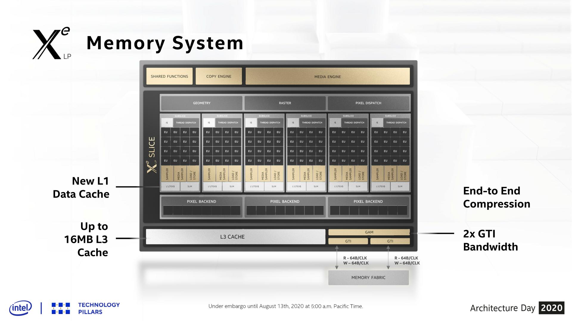
Execution units now work in pairs, rather than on their own, with a thread scheduler shared between each pair. Even with this change, each individual execution unit has moved to an 8+2 wide design, with the first 8 working on FP/INT and the final two on complex math. Previously we saw something more akin to a 4+4 design, so Intel has rebalanced the math engine while also making in larger per unit. This new 8+2 design actually decreases the potential of some arithmetic directly blocking the FP pipes, improving throughput particularly in graphics and compute workloads.
The full Tiger Lake LP solution has all 96 execution units, with six sub-slices each of 16 execution units (6x16), Rocket Lake is neutered by comparison. Rocket Lake has 4 sub-slices, which would suggest a 64 execution unit design, but actually half of those EUs are disabled per sub-slice, and the final result is a 32 EU implementation (4x8). The two lowest Rocket Lake processors have only a 3x8 design. By having only half of each sub-slide active, this should in theory give more cache per thread during operation, and provides less cache pressure. Intel has enabled this flexibility presumably to provide a lift in edge-case graphics workloads for the parts that have fractional sub-slices enabled.
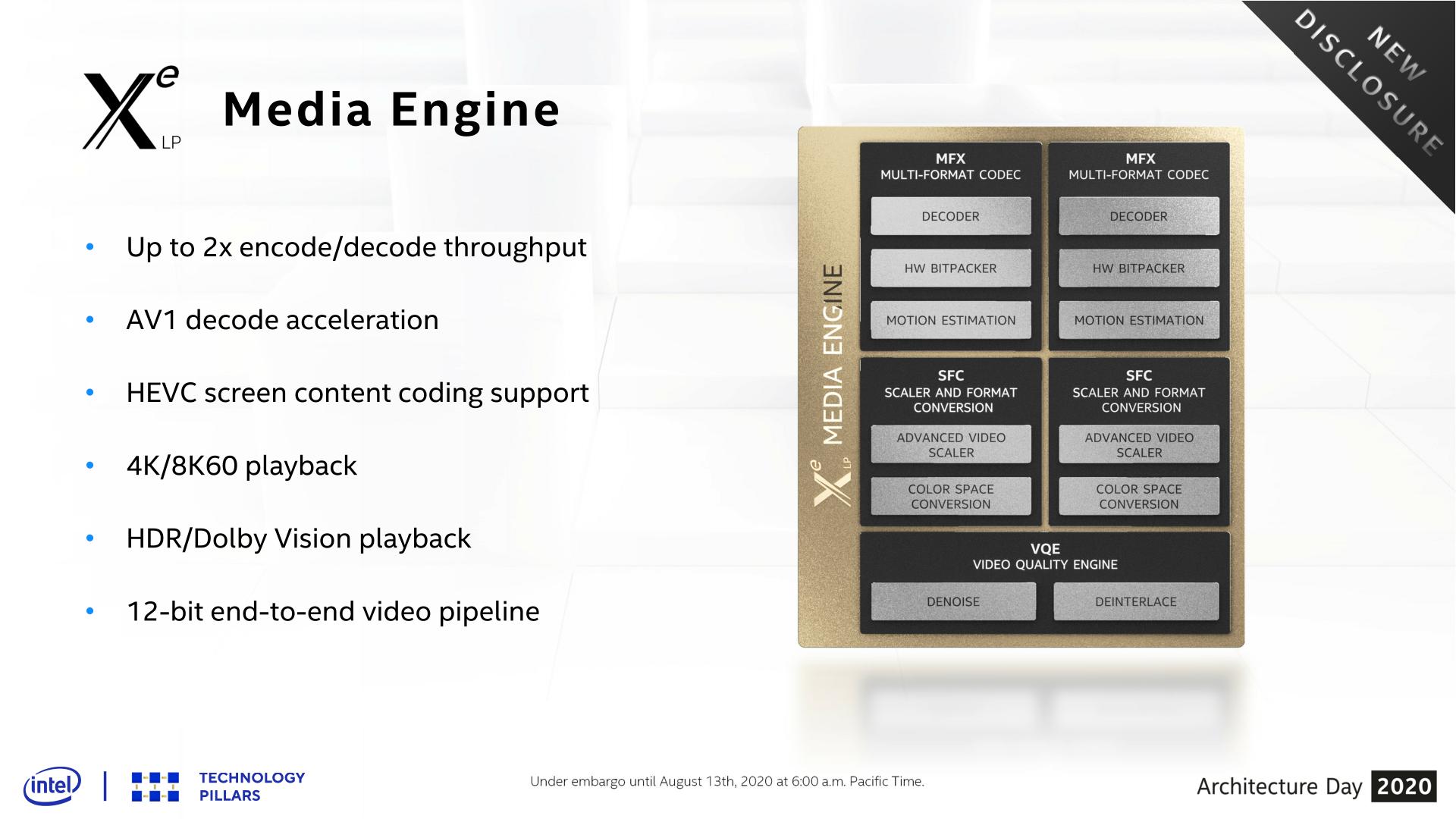
Xe-LP also comes with a revamped media engine. Along with a 12-bit end-to-end video pipeline enabling HDR, there is also HEVC coding support and AV1 decode, the latter of which is a royalty-free codec providing reported similar or better quality than HEVC. Intel is the first desktop IGP solution to provide AV1 accelerated decode support.
Rocket Lake Comparisons
For this review, we are using the Core i9-11900K, Core i7-11700K, and Core i5-11600K. These three are the highest power processors in Intel’s Rocket Lake lineup, and as a result they support the highest configuration of LP graphics that Intel provides on Rocket Lake. All three processors have a 4x8 configuration, and a turbo frequency up to 1300 MHz.
| Intel Integrated Graphics | |||||
| AnandTech | Core i9 11900K |
Core i7 11700K |
Core i5 11600K |
Core i9 10900K |
|
| Cores | 8 / 16 | 8 / 16 | 6 / 12 | 10 / 20 | |
| Base Freq | 3500 MHz | 3600 MHz | 3900 MHz | 3700 MHz | |
| 1T Turbo | 5300 MHz | 5000 MHz | 4900 MHz | 5300 MHz | |
| GPU uArch | Xe-LP | Xe-LP | Xe-LP | Gen 11 | |
| GPU EUs | 32 EUs | 32 EUs | 32 EUs | 24 EUs | |
| GPU Base | 350 MHz | 350 MHz | 350 MHz | 350 MHz | |
| GPU Turbo | 1300 MHz | 1300 MHz | 1300 MHz | 1200 MHz | |
| Memory | DDR4-3200 | DDR4-3200 | DDR4-3200 | DDR4-2933 | |
| Cost (1ku) | $539 | $399 | $262 | $488 | |
Our comparison points are going to be Intel’s previous generation Gen11 graphics, as tested on the Core i9-10900K which has a 24 Execution Unit design, AMD’s latest desktop processors, a number of Intel’s mobile processors, and a discrete graphics option with the GT1030.
In all situations, we will be testing with JEDEC memory. Graphics loves memory bandwidth, and CPU memory controllers are slow by comparison to mobile processors or discrete cards; while a GPU might love 300 GB/s from some GDDR memory, a CPU with two channels of DDR4-3200 will only have 51.2 GB/s. Also, that memory bank needs to be shared between CPU and GPU, making it all the more complex. The use case for most of these processors on integrated graphics will often be in prebuilt systems designed to a price. That being said, if the price of Ethereum keeps increasing, integrated graphics might be the only thing we have left.
The goal for our testing comes in two flavors: Best Case and Best Experience. This means for most benchmarks we will be testing at 720p Low and 1080p Max, as this is the area in which integrated graphics is used. If a design can’t perform at 720p Low, then it won’t be going anywhere soon, however if we can achieve good results at 1080p Max in certain games, then integrated graphics lends itself as a competitive option against the basic discrete graphics solutions.
If you would like to see the full CPU review of these Rocket Lake processors, please read our review:
Intel Rocket Lake (14nm) Review: Core i9-11900K, Core i7-11700K, and Core i5-11600K
Pages In This Review
- Analysis and Competition
- Integrated Graphics Gaming
- Conclusions and Final Words


165 Comments
View All Comments
mode_13h - Sunday, May 9, 2021 - link
Well, obviously "making in larger" should be "making it larger".They mean changing the ratio of ALU pipelines capable of handing different sorts of operations, while also increasing their total number by 25% (i.e. from 4+4 to 8+2, in referring to fp/int + complex operations). And by "complex", presumably they mean things like sqrt, sin, and atan.
watzupken - Friday, May 7, 2021 - link
The results are pretty bad if you ask me. Considering all the hype on the XE graphics, the improvements over last gen UHD graphics isn’t great. When comparing say i9 11900 and 10900, it’s a comparison between a 32 vs 24 EU part. So whatever the results, we need to account for that 30% increase in EUs. At the end of the day, it’s just good for light games and mostly non 3D intensive use.mode_13h - Sunday, May 9, 2021 - link
> Considering all the hype on the XE graphicsThis type of small implementation isn't what the hype was about.
> the improvements over last gen UHD graphics isn’t great.
Yeah, but you're comparing 14 nm to 14 nm and not much more die area. So, I don't know why you were expecting any miracles, here.
> When comparing say i9 11900 and 10900, it’s a comparison between a 32 vs 24 EU part.
> So whatever the results, we need to account for that 30% increase in EUs.
Just eyeballing it, the results well *exceed* that bar, in most cases!
I'm not saying Rocket Lake's iGPU is *good*, just that performs at least as well as one would expect, considering it's still 14 nm and has only 32 EUs.
Spunjji - Monday, May 10, 2021 - link
> Yeah, but you're comparing 14 nm to 14 nm and not much more die area. So, I don't know why you were expecting any miracles, here.According to AT's percentages compared to the actual die sizes, Intel spent roughly an extra 13mm^2 of die area, or about a 28% increase. Performance-per-area has definitely gone up, but it's not a giant leap.
vegemeister - Friday, May 7, 2021 - link
>From Intel, its integrated graphics is in almost everything that Intel sells for consumers. AMD used to be that way in the mid-2010s, until it launched RyzenEh? Bulldozer -- no IGP. Phenom II -- no IGP. The various Athlons -- no IGP as far as I recall.
mode_13h - Sunday, May 9, 2021 - link
Yeah, that was a weird position for them to take.APUs were always a lower-teir product, for AMD.
eastcoast_pete - Friday, May 7, 2021 - link
Conclusion: Let's hope Intel gives Alder Lake at least 96 EU Xe graphics as iGPU; as things look right now, dGPUs will remain unaffordable or downright unobtainable. Otherwise, it's back to 10 fps as standard.mode_13h - Sunday, May 9, 2021 - link
I doubt it. For the desktop market, I'd expect more in the range of 48-64. I think die area currently commands too much of a premium.As Intel has a history of offering bigger iGPUs in some of their laptop chips, I don't see Tiger Lake's 96 EUs as a precedent for what we should expect of their 10 nm desktop processors.
Spunjji - Monday, May 10, 2021 - link
Agreed here. For a vast chunk of their market, it's just not relevant. I doubt we'll see this change much until they start using chiplets, and then we might get the *option* to buy something with a bigger iGPU.TheJian - Saturday, May 8, 2021 - link
Why is the 4750g even in the list if you can't BUILD with it? They are about to launch a new one and you can't even get it until xmas maybe (they say Q3-Q4, but that means Q4) for an actual DIY build.Stop making console socs AMD so you'll have more wafers for stuff that makes NET INCOME. I think there are a few people who'd like some 57xx apu's before xmas and surely they'd make more than single digit or mid-teens margins (meaning <15% right? or you'd say 15!). ~1000mm^2 wasted on every soc gone to consoles and HALF of that is the GOOD wafers that could go to chips that make THOUSANDS not $10-15 each. Just saying...500mil NET again...