AMD Kaveri Review: A8-7600 and A10-7850K Tested
by Ian Cutress & Rahul Garg on January 14, 2014 8:00 AM ESTKaveri and Counting Cores
With the move towards highly integrated SoCs we've seen a variety of approaches to core counts. Apple, Intel and Qualcomm still count CPU cores when advertising an SoC. For Apple and Qualcomm that's partially because neither company is particularly fond of disclosing the configuration of their GPUs. More recently, NVIDIA took the somewhat insane stance of counting GPU CUDA cores on its Tegra K1 SoC. Motorola on the other hand opted for the bizarre choice of aggregating CPU, GPU and off-die companion processors with the X8 platform in its Moto X smartphone. Eventually we will have to find a way to characterize these highly integrated SoCs, particularly when the majority of applications actually depend on/leverage both CPU and GPU cores.
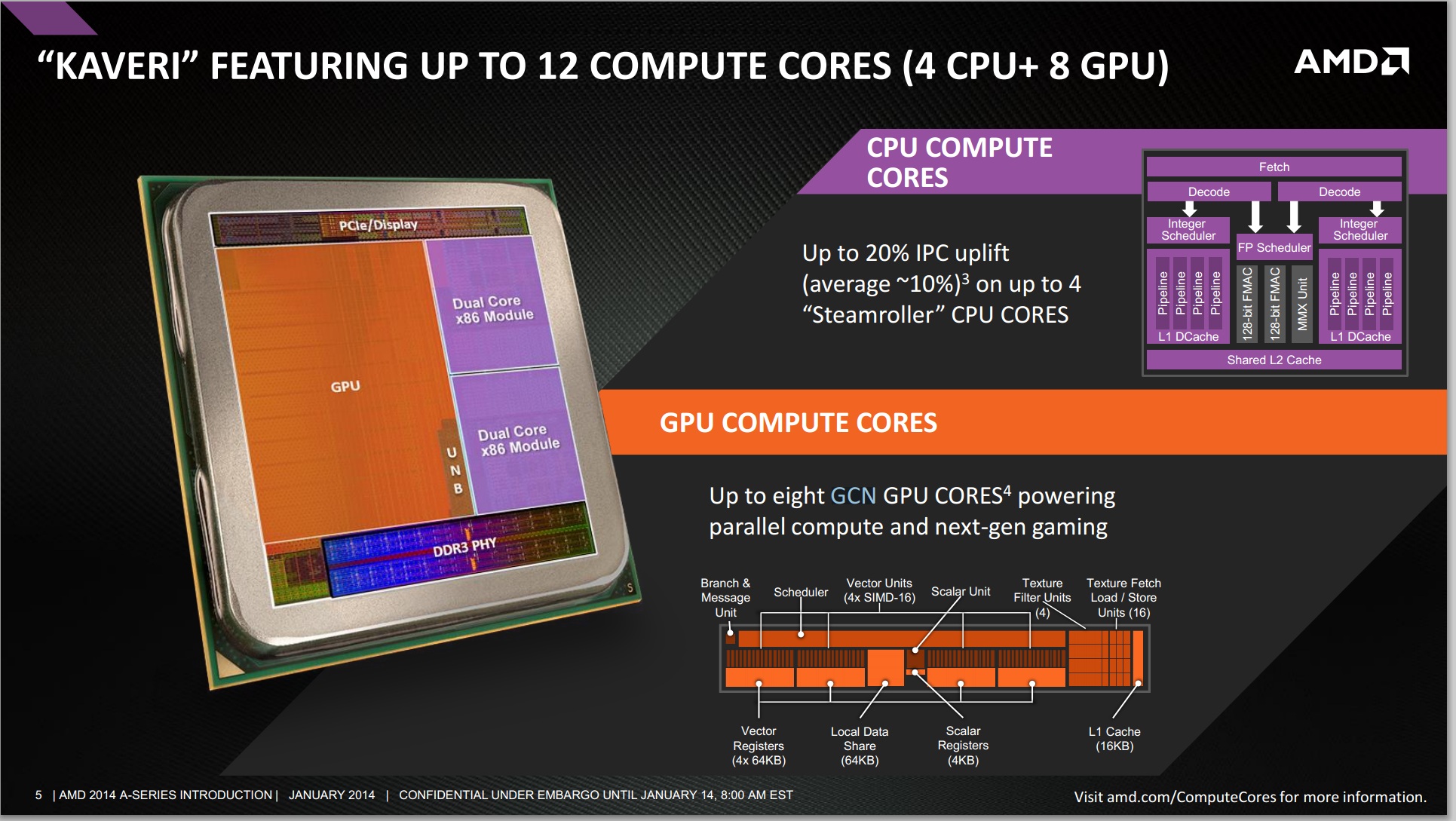
AMD finds itself in a unique position with Kaveri where it has a truly unified CPU/GPU architecture and needs to establish a new nomenclature for use in the future. With 47% of the Kaveri die dedicated for GPU use, and an architecture that treats both CPU and GPU as equals, I can understand AMD's desire to talk about the number of total cores on the APU.
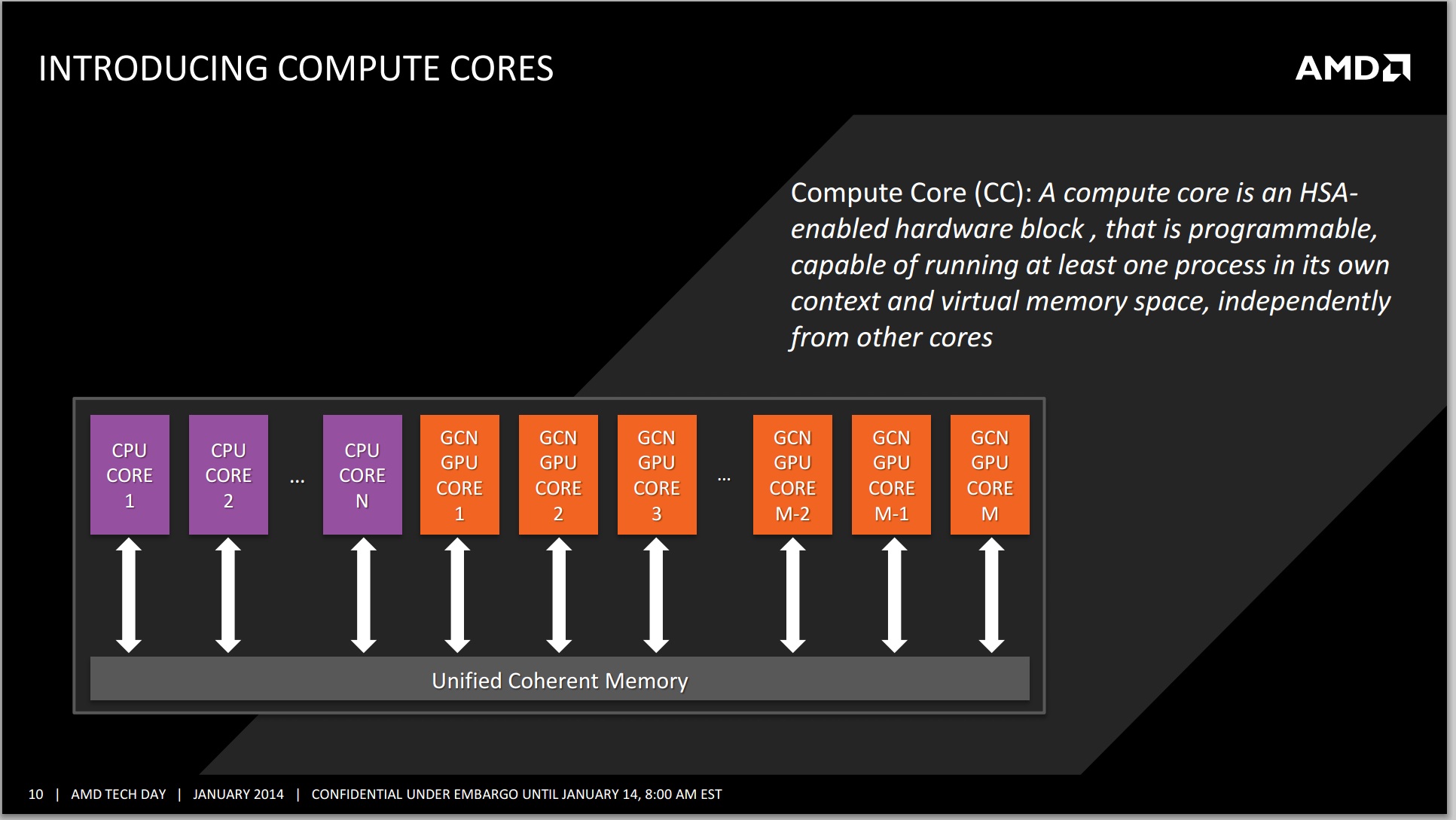
AMD settled on the term "Compute Core", which can refer to either an x86 (or maybe eventually ARM) CPU core or a GCN compute unit. The breakdown is as follows:
- Each thread on a CPU is a Compute Core
- Each Compute Unit on the IGP is a Compute Core
- Total Compute Cores = CPU Compute Cores + IGP Compute Cores
This means that the high end SKU, the A10-7850K will have a total of 12 compute cores: four from the CPU (two Steamroller modules supporting four threads) and eight from the IGP (due to eight compute units from the R7 graphics).
There are some qualifications to be made on this front. Technically, AMD is correct – each compute unit in the IGP and each thread on the CPU can run separate code. The Hawaii GCN architecture can spawn as many kernels as compute units, whereas a couple of generations ago we were restricted to one compute kernel on the GPU at once (merely with blocks of work being split across the CUs). However, clearly these 12 compute units are not equivalent: a programmer will still have to write code for the CPU and GPU specifically in order to use all the processing power available.
Whenever AMD (or partners) are to promote the new APUs, AMD tells us clearly that two sets of numbers should be quoted in reference to the Compute Cores – the total, and the breakdown of CPU/GPU on the APU. Thus this would mean that the A10-7850K APU would be marketed at a “12 Compute Core” device, with “(4 CPU + 8 GPU)” following immediately after. I applaud AMD's decision to not obfuscate the internal configuration of its APUs. This approach seems to be the most sensible if it wants to tout the total processing power of the APU as well as tell those users who understand a bit more what the actual configuration of the SoC is. The biggest issue is how to address the users who automatically assume that more cores == better. The root of this problem is very similar to the old PR-rating debates of the Athlon XP. Explaining to end users the intracacies of CPU/GPU programming is really no different than explaining why IPC * frequency matters more than absolute frequency.
When a programmer obtains an APU, the OpenCL profiler should locate the eight compute units of the GPU and display that to the user for offloading compute purposes; at the same time it is up to the programmer to leverage the threads as appropriately as possible, even with AMD’s 3rd generation Bulldozer modules implementing a dual-INT + single-FP solution.
At launch, AMD will offer the following configurations:
- A10-7850K: 12 Compute Cores (4 CPU + 8 GPU)
- A10-7700K: 10 Compute Cores (4 CPU + 6 GPU)
- A8-7600: 10 Compute Cores (4 CPU + 6 GPU)
The problem with distilling the processing power of the APU into a number of compute cores is primarily on the CPU side. AMD will be keeping the GPU at approximately the same clock (720 MHz for these three) but the CPU frequency will differ greatly, especially with the A8-7600 which has configurable TDP and when in 45W mode will operate 300-400 MHz less.
Steamroller Architecture Redux
We've already documented much of what Steamroller brings to the table based on AMD's Hot Chips presentation last year, but I'll offer a quick recap here.
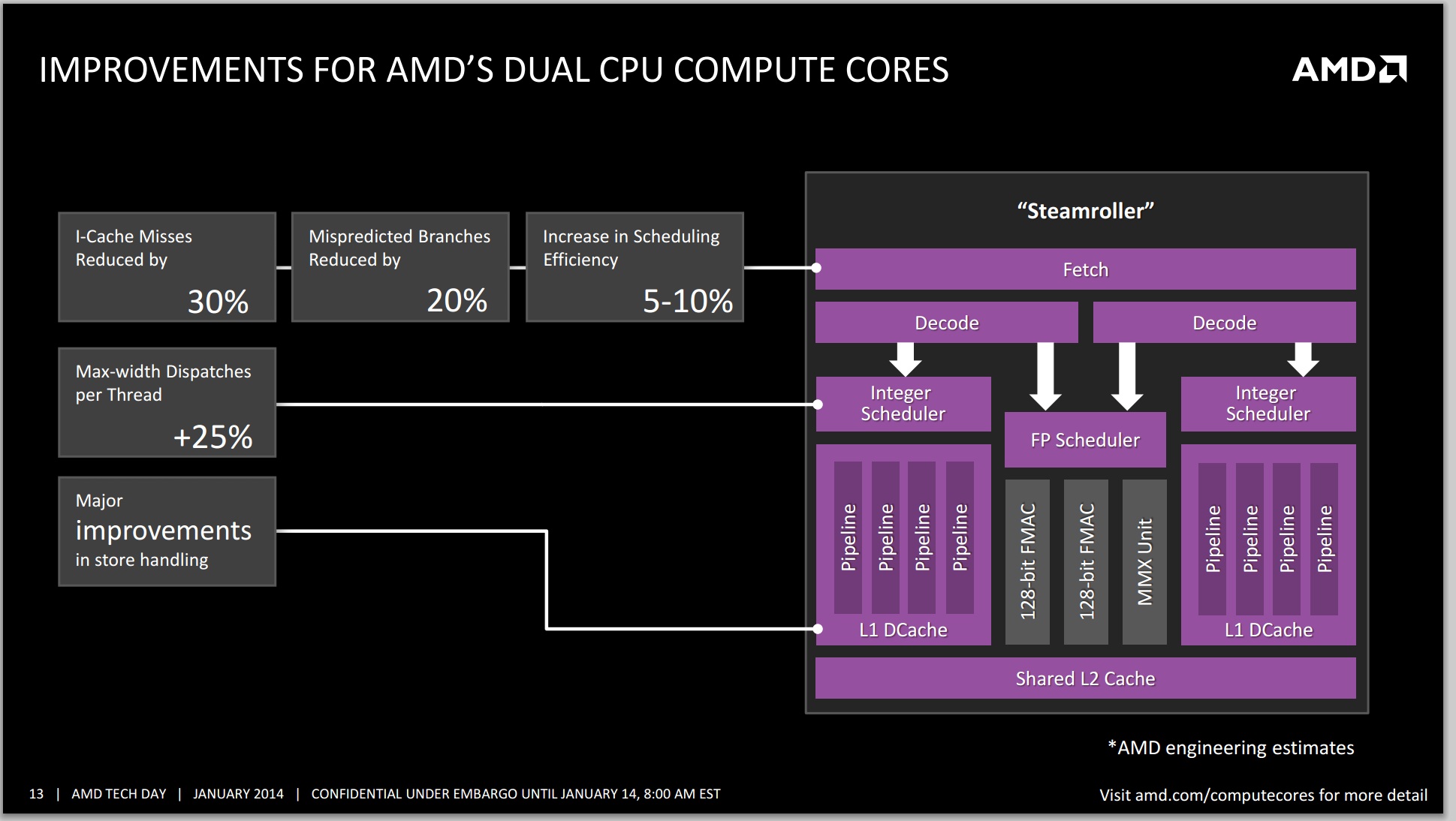
Steamroller brings forward AMD's Bulldozer architecture, largely unchanged. We're still talking about a dual-core module featuring two independent integer execution cores with a single shared floating point execution core capable of executing instructions from two threads in parallel. A single module still appears as two cores/threads to the OS.
In Bulldozer and Piledriver, each integer core had its own independent scheduler but the two cores shared a single fetch and decode unit. Instructions would come in and decodeded operations would be fed to each integer pipe on alternating clock cycles. In Steamroller the decode hardware is duplicated in each module, so now each integer core gets its own decode unit. The two decode units are shared by the one FP unit.
L1 instruction caches increase in size from 64KB to 96KB per module, which AMD claims reduces misses by up to 30%. There's an updated branch predictor which is responsible for reducing mispredicted branches by up to 20%. Both integer and FP register files grow in size as well as an increase in the size of the scheduling window, a combination of which increases the number of dispatches per thread by up to 25%.
There are huge improvements on the store side. Steamroller can now issue up to 2 stores at the same time compared to 1 in Bulldozer/Piledriver. The load/store queue sizes go up by around 20% as well. It's remarkable just how much low hanging fruit there was in the Bulldozer design.
GCN in an APU
The integrated graphics solution on Trinity/Richland launched with a Cayman-derived VLIW4 architecture, which unfortunately came just shortly after desktop side of the equation finished moving from VLIW5/VLIW4 to GCN. Having a product stack with largely different GPU architectures doesn't help anyone, particularly on the developer front. Looking forward, sticking with GCN was the appropriate thing to do, as now Kaveri is using GCN, the same architecture found in AMD’s high end R9-290X GPU, based on the Hawaii platform.
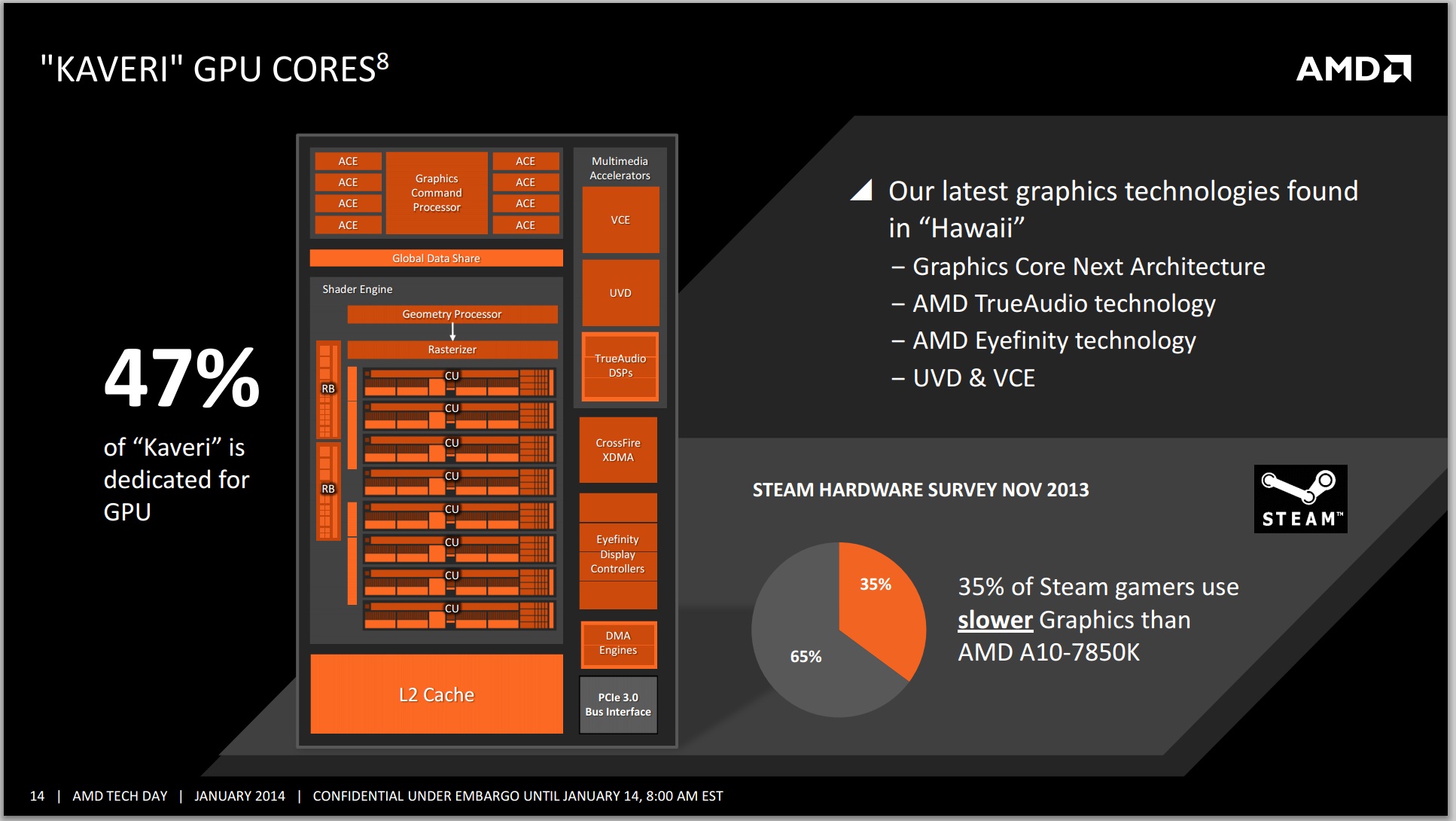
This enabled AMD to add in all the features they currently have on Hawaii with little to no effort – the TrueAudio DSP, the upgraded Video Coding Engine and Unified Video Decoder are such examples. Whether or not AMD decides to develop an APU with more than 8 GCN CUs is another matter. This is a point we've brought up with AMD internally and one that I'm curious about - do any AnandTech readers have an interest in an even higher end APU with substantially more graphics horsepower? Memory bandwidth obviously becomes an issue, but the real question is how valuable an Xbox One/PS4-like APU would be to the community.


380 Comments
View All Comments
PolarisOrbit - Tuesday, January 14, 2014 - link
In the GPU benchmarks the charts were all divided into categories "Performance," "Quality," and "Xtreme." I went back to Testing Platform page to discern what these meant but it didn't say. Any clues?Ryan Smith - Tuesday, January 14, 2014 - link
Check the first page of the GPU performance section; it goes over the different categories.Th-z - Tuesday, January 14, 2014 - link
Nice review and very nice info from Rahul. Questions and comments:1. Not sure why you guys think this should be called SoC. Its MB still has a southbridge and other components to make a complete system.
2. Page 2, first paragraph: "Apple’s Mac Pro dream" and "by doing the dream on a single processor". What is the "dream" you are referring to?
3. Page 9, Table "Intel TestBed", i7s should be 4C/8T.
4. Don't you guys think it's odd that how close 95 W A10-7850K compares to 65 W A8-7600 and 45 W A8-7600 in gaming? With 33.3% more SP, it should have more noticeable increase in FPS. We see better spread with Richland, yet all three of Kaveri are so close to each other, which really makes 7850K unattractive with more than double the TDP compares to 7600 at 45 W.
Could it be it may have been bottlenecked by memroy bandwidth? Sooner or later AMD would need to do their own embedded RAM or putting GDDR5 on MB -- the world's first user configurable GDDR5 on MB, that would be something.
T1beriu - Tuesday, January 14, 2014 - link
4. Could it be because all of them have the same 512 core GPU clocked at the same speed of 720Mhz?T1beriu - Tuesday, January 14, 2014 - link
Nope, I'm just blind.ws3 - Tuesday, January 14, 2014 - link
The Iris Pro results have got to be very worrying for AMD.Yes, Intel is still behind in integrated graphics, but they are improving by leaps and bounds, and their CPU performance is miles ahead of AMD.
I loved my Athlons, but I think AMD is on the verge of having nothing to offer.
UtilityMax - Tuesday, January 14, 2014 - link
Iris Pro is basically a proof that Intel can respond to AMD if the APU market does take off. Right now Iris Pro graphics are too expensive, but they could eventually move it onto the same die shared with a lower end i3 CPU.thomascheng - Wednesday, January 15, 2014 - link
AMD already proven they can make a bigger core. Just look at the PS4 and Xbox One. I think while Intel can have the performance crown, only a small percentage will actually buy it.andrewaggb - Wednesday, January 15, 2014 - link
The shame is that AMD should have released an APU similiar to the Pro. They have the tech, the drivers, mantle coming, the gaming deals... to actually pull it off. The biggest problem with iris pro (besides price) is that intel drivers suck. AMD drivers (at least in single gpu scenerios) work well. I think releasing cheap apu's is a good move as well, but at least one high end model would have been good. I think it would sell reasonably well if it could get 60fps at 1080p (ps4 level perf). I don't even think it has to be all that cheap, should be worth at least $100 premium. It enables new possibilities and smaller/quiter form factors. People like that.khanov - Tuesday, January 14, 2014 - link
As you hinted at several times in your article, I think we could see even better iGPU performance from Kaveri with increasing memory bandwidth. I wonder if you might be interested in benchmarking some games at different memory frequency settings up to (and beyond?) DDR3-2400?I personally was hoping that Kaveri might launch with a quad-channel DDR3 memory controller. Yes it would require a new socket and the added signal routing complexity would push up board prices a bit. However, as FM2+ boards are so cheap, I don't see that as a big issue really.
You also asked if anyone would be interested in a XBox One/PS4 style APU with significantly more GPU cores. Well I would! But again, that memory bandwidth issue needs to be resolved.
Something like a six layer mini ITX board with 8GB of GDDR5 soldered underneath (where else would there be room to put it?) would be the brilliant if coupled with a PS4 style APU. It's a nice dream.
Thanks for the very in-depth review. It was a pleasure to read.