Examining Intel's Ice Lake Processors: Taking a Bite of the Sunny Cove Microarchitecture
by Dr. Ian Cutress on July 30, 2019 9:30 AM EST- Posted in
- CPUs
- Intel
- 10nm
- Microarchitecture
- Ice Lake
- Project Athena
- Sunny Cove
- Gen11
Combining 10nm CPU + 14nm Chipset
As with Intel’s previous low-power (sub 28W) mobile designs, the company will be combining the CPU and the chipset onto a single package. This typically helps in enabling a smaller motherboard design for thin and light systems that might want to dedicate that area to additional battery, or simply save the footprint altogether. The flip side is that there are more pin-outs, and the board design has to be suitable for the increased signal traces, but this is nothing new. For Ice Lake-U, Intel has stated that the CPU, which is being built on their second-generation 10nm "10+" process, will be paired with a new generation ‘14nm class’ chipset.
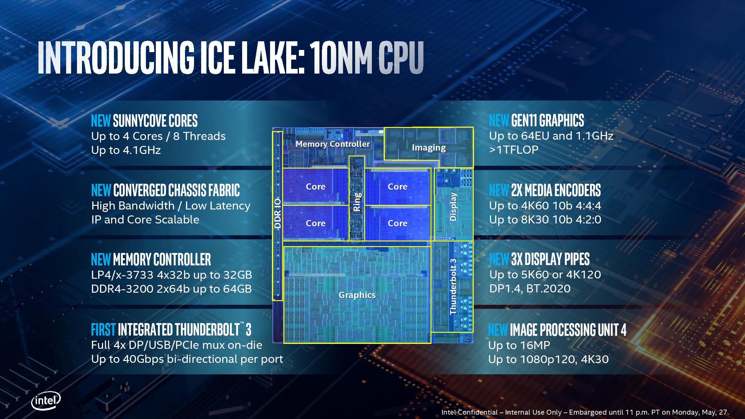
As stated on the previous page, the CPU will offer up to four cores, eight threads, go up to 4.1 GHz, provide integrated TB3 (more on that later), and a vast improvement to the graphics capabilities (also more on that later).
One of the big updates to the design will be enabling support for both DDR4 and LPDDR4/LPDDR4X on a single memory controller. Up until this point, only Intel’s latest Atom designs had LPDDR4 enabled, so this is a welcome addition to the main high-performance product line. In this instance Intel will support LPDDR4/X with up to four 32-bit channels at 3733 MT/s for 32 GB, or if a user needs more capacity, up to 64GB of DDR4-3200 with two 64-bit channels. The LPDDR4/X implementation will allow for lower idle power states, saving power and battery life when the memory is not in use, however it does this in exchange for maximum capacity. It’s an interesting tradeoff for sure. The peak power consumption of both modes in an equally populated system, given the respective frequency difference, should be similar.
One element that Intel hasn’t talked about is its ‘new converged chassis fabric’, which we believe to be a scalable power and environment control fabric that connects between chips in order to both transfer data but also to manage how and where power is applied within a system. The fact that Intel calls this ‘IP and Core scalable’ suggests that if vendors want to add additional supported chips to the system, say for example a future Intel AI chip, that might be possible and it could be controlled through this fabric. It will be interesting to see if Intel divulges any more of this information.
Not mentioned in this slide are the new performance enhancements, such as AVX-512 and other new instructions, which we’ll cover in detail a bit later.
The connection to the chipset is through a DMI 3.0 x4 link, as with current generations of Intel products.
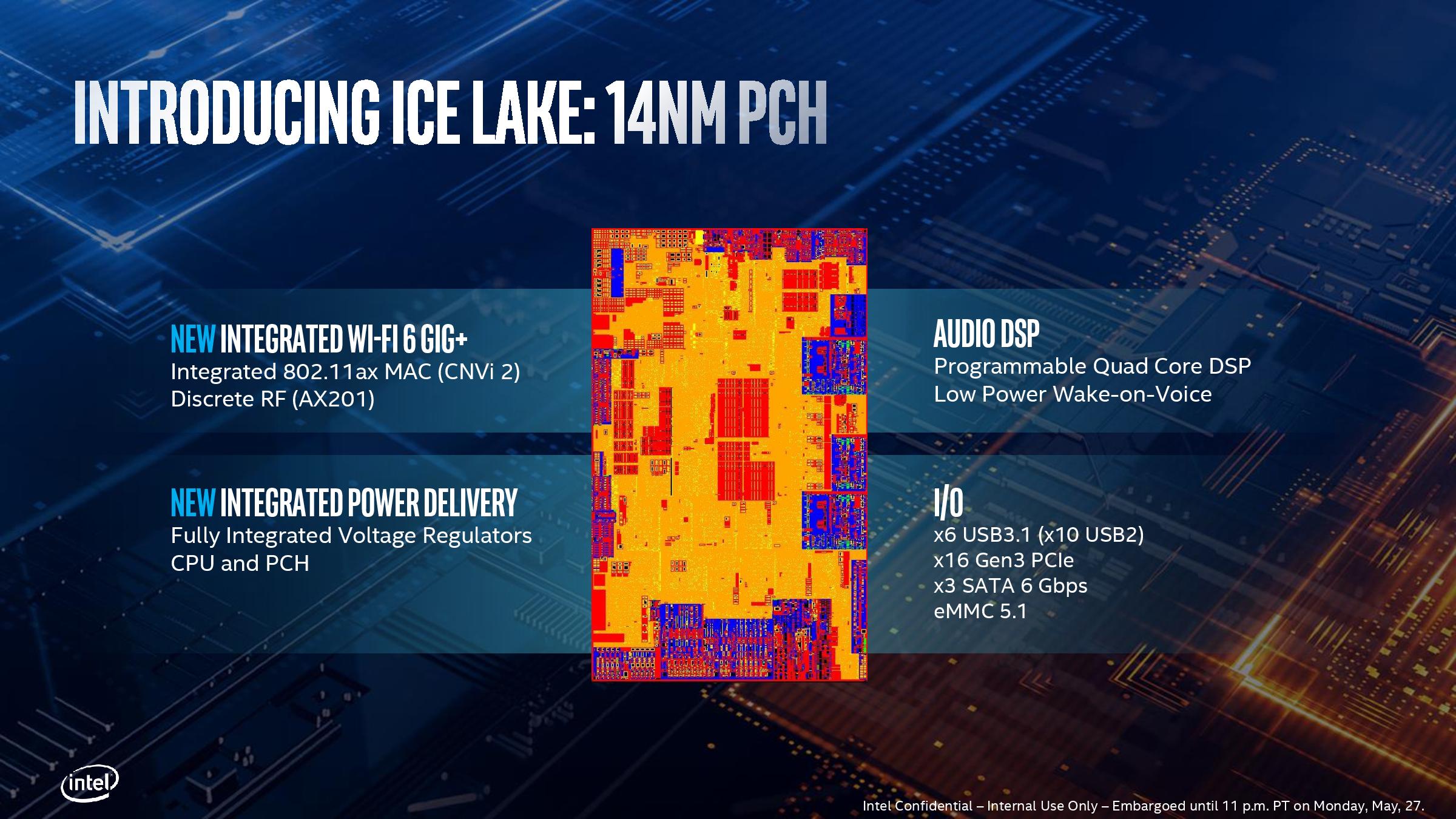
The new ‘14nm class’ chipset is also an update from Intel’s 8th Gen Core mobile processors. It does not yet have a series designation, but given the updates, this is likely to be a member of the 400-series chipset line.
With the new chipset, Intel has updated the proprietary CNVi protocol on the die to support CNVi 2, which is found on the latest Wi-Fi 6 Intel-Only RF modules, such as AX201. This update to a second generation implementation is likely to be for throughput reasons, given the increased bandwidth that Wi-Fi 6 provides over Wi-Fi 5.
Intel also promotes better integrated power delivery on the chipset, meaning that the PCH can share the same power rail as the CPU, reducing the number of on-board components inside the mobile system. This should reduce cost, and hopefully the thermal density of the power delivery onboard the chip doesn’t have a negative effect. Also on the power side, Intel states that the audio DSP on the chipset has also been improved for lower power operation.
On the IO side of the chipset, Ice Lake will support up to six ports of USB 3.1 (which is now USB 3.2 Gen 1 at 5 Gbps), or 10 USB 2.0 ports, or a mix. There are also 16 HSIO lanes which are broadly presented as PCIe 3.0, although given previous HSIO models it is likely that certain combinations of ports will be required for specific features. However this should afford at least two, if not three, potential PCIe 3.0 x4 NVMe drives in these systems. For SATA, there is access to three direct ports, but there is also an eMMC 5.1 link. Intel does not state if UFS is supported for super-small form factor systems.
Ice Lake is not Intel’s first crack at 10nm
We documented the history of Intel’s 10nm process with our review of the first 10nm CPU to come from the company. Our Core i3-8121U analysis of the Cannon Lake design is one Intel would rather forget – the manufacturing process didn’t yield, the frequency wasn’t there, the power consumption was too high, and the graphics were completely fused off. But hey, Intel still shipped it to customers by the end of 2017, and it found its way into some Chinese educational notebooks, and some NUCs, eventually, satisfying promises made to shareholders.

Fast forward almost 18 months, and we’re about to see Intel’s second take on 10nm with Ice Lake. Under Intel’s nomenclature, Ice Lake is technically being built with the ‘10+’ process, which is meant to be an improved version of the 10nm used in Cannon Lake. The fact that parts of the CPU are now working means that it earns that plus. Intel pointed to an extra metal layer (going from 12 to 13) in the manufacturing has helped with power delivery and frequency, and new transistor library designs and MIM caps have helped with voltages. Intel is also using a thin magnetic inductor array, and a recess in motherboard design for reduced package z-height.
As for Intel’s future, the company has stated at events that it is now developing future process nodes with these ‘BKM’ updates built into the lifecycle of the process node, such as 10+ and 10++ as part of the family of 10nm processes, and then beyond to 7nm with 7, 7+, and 7++ over the next few years. It’s worth noting that while Intel has officially shipped a first generation 10nm product, is promoting Ice Lake as a ‘10+’ second generation 10nm product, and has specified a number of 10nm class products up and down its product portfolio, we are still waiting on an official presentation about how Intel’s 10nm process works in a formal setting, rather than bits and pieces from events like ISSCC and IEDM. What we have pieced together from those events is likely out of date for 10+, however we do know that for 10nm Intel has three different libraries based on performance, each with different transistor densities: from 67 million transistors / mm2 for ultra-high performance, to 101 million transistors / mm2 for high-density logic. You can read more about it here.


107 Comments
View All Comments
name99 - Wednesday, July 31, 2019 - link
That’s an idiotic chain of reasoning.ARM Macs will ship with macOS, not iOS. To believe otherwise only reveals that you know absolutely nothing of how Apple thinks.
As for comparison, the rough number is A12X gets ~5200 on GB4, Intel best (non-OC’d) gets ~5800. That’s collapsing lots of numbers down to one, but comparing benchmark by benchmark you see Apple does very well (almost matching Intel) across an awful lot.
If Apple can maintain its past pace (and there is no reason why not...) we can expect A13X to be anywhere from 20% to 35% faster, which puts it well into “fastest [non-OC’d] CPU on earth” territory for most single-threaded use cases. Can they achieve this? Absolutely.
Just process improvement can get them 10% frequency. I expect A13X to clock around 2.8GHz.
Then there is LPDDR5 which I expect they will be using, so substantially improved memory bandwidth. Then I expect they'll have SVE (2x256) and accompanying that basically double the bandwidth all the way out from L1 to DRAM.
These are just the obvious basics. There are a bunch of things they can still do that represent “fairly easy” improvements to get to that 25% or so. (These include more aggressive fusion, a double-pumped ALU, attached ALUs to load/store to allow load-ok and op-store fusion, a micro-op cache, long-term-parking, criticality prediction, ...)
So, if it’s so easy, why doesn’t Intel also do it? Why indeed? That’s why I occasionally post my alternative rant about how INTC is no longer an engineering company, it is now pretty much purely a finance company...
ifThenError - Friday, August 2, 2019 - link
Sorry, but both these comments seem mighty uninformed. The MacBooks Air and Pro currently and in the foreseeable future all run on Intel CPUs. The Apple Chips A12/13 are used in iPhone, iPad and the likes.And regarding your prediction, your enthusiasm seems way over the top. What are you even talking about? Micro-op cache on a RISC processor? Think again. Aren't RISC commands all micro ops already?
name99 - Sunday, August 4, 2019 - link
Strong the Dunning-Kruger is with this one...Dude, seriously, learn something about MODERN CPU design, more than just buzz-words from the 80s.
To get you started, how about you read
https://www.anandtech.com/show/14384/arm-announces...
and concentrate on understanding EVERY aspect of what's being added to the CPU and why.
Note in particular that 1.5K Mop cache...
More questions to ask yourself:
- Why was 80s RISC obsessed with REDUCED instructions?
- Why was ARM (especially ARMv8) NOT obsessed with that? Look at the difference between ARMv8 and, say, RISC-V.
- Why is op-fusion so important a part of modern high performance CPUs (both x86 and ARM [and presumably RISC-V if they EVER ship a high-performance part, ha...])?
- which are the fast (shallow logic, even if it's wide) and which are the slow (deep logic) parts of a MODERN pipeline?
ifThenError - Monday, August 5, 2019 - link
Oh my, this is so entertaining you should charge for the reading.You demand to go beyond just buzz words (what would be good) while your posts look like entries to a contest on how many marketing phrases can be fit into a paragraph.
Then you even manage to combine this with highly rude idiom. Plus you name a psychological effect but fail to transfer it to self-reflexion. And as cherry on the top you obviously claim for yourself to understand „EVERY aspect“ of a CPU (an unimaginably complex bit of engineering) but even manage to confuse micro- and macro-op cache and the conceptual differences of these.
I'm really impressed by your courage. Publicly posting so boldly on such a thin basis is brave.
Your comments add near zero information but are definately worth the read. Pure comedy gold!
Please see this as an invitation to reply. I'm looking forwards to some more of your attempts to insult.
Techgeek43 - Tuesday, July 30, 2019 - link
Fantastic article Ian, I for one, cannot wait for ice lake laptopsWonderful in-depth analysis, with an interesting insight into the Intel brand
repoman27 - Tuesday, July 30, 2019 - link
"The high-end design with 64 execution units will be called Iris Plus, but there will be a ‘UHD’ version for mid-range and low-end parts, however Intel has not stated how many execution units these parts will have."Ah, but they have: Ice Lake-U Iris Plus (48EU, 64EU) 15 W, Ice Lake-U UHD (32EU) 15 W. So their performance comparisons may even be to the 15 W Iris Plus with 64 EUs, rather than the full fat 28 W version.
I know you have access to the media slide decks, but Intel has also posted product briefs for the general public that contain a lot of this info: https://www.intel.com/content/www/us/en/products/d...
"On display pipes, Gen11 has access to three 4K pipes split between DP1.4 HBR3 and HDMI 2.0b. There is also support for 2x 5K60 or 1x 4K120 with a 10-bit color depth."
The three display pipes are not limited to 4K, and are agnostic of transport protocol—each of them can be output via the eDP 1.4b port, one of the 3 DDI interfaces which can support either DisplayPort 1.4 or HDMI 2.0b, or one of the up to 4 Thunderbolt 3 ports. Both HDMI and DP support HDCP 2.2, and DisplayPort also supports DSC 1.1. The maximum single pipe, single port resolution for HDMI is 4K60 10bpc (4:2:2), and for DisplayPort it's 4K120/5K60 10bpc (with DSC).
Thunderbolt 3 integration for Ice Lake-Y is only up to 3 ports.
abufrejoval - Tuesday, July 30, 2019 - link
What I personally liked most about the GT3e (48 EU) and GT4e (72 EU) Skylake variant SoCs was, that they didn't cost the extra money they should have, especially when you consider that the iGPU part completely dwarfs the CPU cores (which Intel makes you bleed for) and is much better than everything else combined together (have a look at the WikiChips layoutshttps://en.wikichip.org/wiki/intel/microarchitectu...
Of course, a significantly better graphics performance is never a bad thing, especially when it also doesn't cost extra electrical power: The bigger iGPUs might have actually been more energy efficient than their GT2 brethren at a graphics load that pushed the GT2 towards its frequency limits. And in any case if you don't crunch it on graphics, the idle consumption is near perfect: One of the reasons most laptop dGPU designs won't even bother to run 2D on the dGPU any more but leave that to Intel.
The biggest downside was that you couldn't buy them outside an Apple laptop or Intel NUC.
But however much Intel goes into Apple mode (the major customer for these beefier iGPUs) in terms of "x time faster than previous", the result aren't going to turn ultrabooks with this configuration into "THD gaming machines".
To have a good feel as to where these could go and whether they are worth the wait, just have a look at the Skull Canyon nuc6i7kyk review on this site: That SoC uses 72 EUs and 128MB of eDRAM and should put a pretty firm upper limit to what a 64 EU Ice Lake can do: Most of the games in that review are somewhat dated yet fail to reach 20FPS at THD.
So if you want to game on the device, you'd be much better of with a dGPU however small and chose the smallest iGPU variant available. No reason to wait, Whisky + Nvidia will do better.
If you want real gaming performance, you need to put real triple digit Watts and the bandwidth only GDDR5/6 or HBM can deliver to work even at THD, but with remote gaming perhaps it doesn't have to be on your elegant slim ultrabook. There again anything but the GT2 configuration is wasted, because only need the VPU part for decoding Google Stadia (or Steam Remote) streams, which is the same for all configurations.
For some strange reason, Intel has been selling GT3/4 NUCs at little or no premium over GT2 variants and in that case I have been seriously tempted. And only once I even managed to find a GT3e laptop once for a GT2 price (while the SoC is literally twice as big and the die carrier even adds eDRAM at zero markup), which I stil cherish.
But if prices are anywhere related to the surface area of the chip (as they are for the server parts), these high powered GTs are something that only Apple users would buy.
That's another reaons, I (sadly) don't expect them to be sold in anything bug Macs and some NUCs, no ChuWi notebooks or Mini-ITX boards.
abufrejoval - Tuesday, July 30, 2019 - link
...(need edit)Judging from the first 10nm generation, GPUs where the part where obtaining economically feasible yields didn't work out. Unless they have really, really fixed 10nm it's not hard to imagine that Intel could be selling high-count EU SoCs to Apple below cost, to keep them for another generation as flagship customer and perhaps due to long-term contractual obligations.
But maintaining GT2/3/4 price egality for the rest of the market seems suicidal even if you have a fab lead.
Not that I expect we'll ever be told: In near monopoly situations the so called market ecnomy becomes surprisingly complex.
willis936 - Wednesday, July 31, 2019 - link
What the hell is a THD in this context?jospoortvliet - Monday, August 5, 2019 - link
Probably full HD (True HD)?