Samsung Kicks Off DDR5 DRAM Production on 12nm Process Tech, DDR5-7200 in the Works
by Anton Shilov on May 18, 2023 7:00 PM EST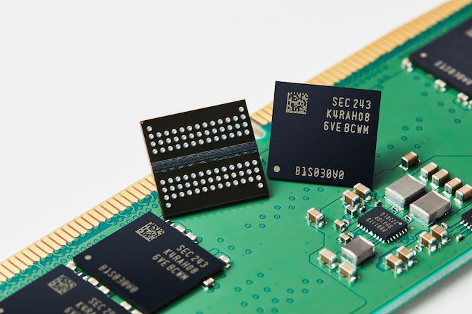
Samsung on Thursday said it had started high volume production DRAM chips on its latest 12nm fabrication process. The new manufacturing node has allowed Samsung to reduce the power consumption of its DRAM devices, as well as decrease their costs significantly compared to its previous-generation node.
According to Samsung's announcement, the company's 12nm fabrication process is being used to produce 16Gbit DDR5 memory chips. And while the company is already producing DDR5 chips with that capacity (e.g. K4RAH086VB-BCQK), the switch to the newer and smaller 12nm process has paid off both in terms of power consumption and die size. As compared to DDR5 dies made on the company's previous-generation node (14nm), the new 12nm dies offer up to 23% lower power consumption, and Samsung is able to produce 20% more dies per wafer (i.e., the DDR5 dies are tangibly smaller).
Samsung says that the key innovation of its 12nm DRAM fabrication process is usage of new high-k material for DRAM cell capacitors that enabled it to increase cell's capacitance to boost performance, but without increasing their dimensions and die sizes. Higher DRAM cell capacitance means a DRAM cell can store more data and reduce power-draining refresh cycles, hence increasing performance. However, larger capacitors typically result in increased cell and die size, which makes the resulting dies more expensive.
DRAM makers have been addressing this by using high-k materials for years, but finding these materials is getting trickier with each new node as memory makers also have to take into account yields and production infrastructure they have. Apparently, Samsung has succeeded in doing so with its 12nm node, though it does not make any disclosures on the matter. That Samsung has succeeded in reducing their die size by a meaningful amount at all is quite remarkable, as analog components like capacitors were some of the first parts of chips to stop scaling down further with finer process nodes.
In addition to introducing a new high-k material, Samsung also reduced operating voltage and noise for its 12nm DDR5 ICs to offer a better balance of performance and power consumption compared to predecessors.
One of the aspects about Samsung's 12nm DRAM technology is that it looks to be the company's 3rd Generation production node for memory that uses extreme ultraviolet lithography. The first D1x node was purely designed as a proof of concept and its successor D1a, which has been in use since 2021, used EUV for five layers. Meanwhile, it is unclear to what degree Samsung's 12nm node is using EUV tools.
"Using differentiated process technology, Samsung’s industry-leading 12nm-class DDR5 DRAM delivers outstanding performance and power efficiency," said Jooyoung Lee, Executive Vice President of DRAM Product & Technology at Samsung Electronics.
Meanwhile, Samsung is also eyeing faster memory speeds with their new 12nm DDR5 dies. According to the company, these dies can run as fast as DDR5-7200 (i.e. 7.2Gbps/pin), which is well ahead of what the official JEDEC specification currently allows for. The voltage required isn't being stated, but if nothing else, it offers some promise for future XMP/EXPO memory kits.
Source: Samsung


18 Comments
View All Comments
meacupla - Thursday, May 18, 2023 - link
The information you want is all there in the article.- Samsung is getting 20% more production per wafer, so that should give you a hint as to if this is really a die shrink or not.
- Capacitors are very difficult to shrink, which is why they lag behind processors
Now as for why you need capacitors in DRAM: How do you think DRAM holds its data? The capacitors provide energy to the DRAM cell. DRAM has to do this over many clock cycles. Processors do not.
The tricky part is shrinking a capacitor without reducing its effectiveness. To get the same amount of energy from a smaller volume, you would need more energy density.
And it would seem Samsung has found a material that allows more density than the previous best that was used in DDR5-4800 chips.
DDR5-4800 chips from Samsung use 17nm, and have a slightly larger die size than Micron DDR5-4800 fabricated on 16nm. SK Hynix uses a 16.5nm node, but it's essentially the same die size, and bit density as Samsung 17nm
Skeptical123 - Friday, May 19, 2023 - link
"The capacitors provide energy to the DRAM cell" capacitors are what stores the actual data. Capacitors might power everything but that's not relevant to this story nor what anyone is talking about."DRAM is a type of random-access semiconductor memory that stores each bit of data in a memory cell, usually consisting of a tiny capacitor and a transistor" - Wikipedia
meacupla - Friday, May 19, 2023 - link
Capacitors are difficult to shrink without reducing their effectiveness, and processors don't use capacitors.How is that not relevant?
tygrus - Monday, May 22, 2023 - link
The capacitors are made in/on the silicon/layers not separate components. The capacitors will leak & the more you shrink them, the higher rate of leakage in proportion to capacity. You can shrink the logic but the capacitors won't shrink linearly with transistor size. Higher voltage & current of signalling to interface with CPU via long tracks need larger transistors than other logic. So you can use a smaller fab node but not all features can be shrunk at the same rate.Analogy: So instead of colouring a large area with a broad brush, color the same area with a smaller brush but you get no benefits except it costs more per m^2. YMMV.
Pneumothorax - Sunday, May 21, 2023 - link
Any insight on why Micron is the worst at DDR5 speed scaling, Samsung is a bit better, while SK Hynix is the undisputed speed king in this gen?meacupla - Monday, May 22, 2023 - link
My best guess is SK hynix has the better, or more robust design when overclocking.you can see the memory die here, although the pictures are a bit small.
https://www.techinsights.com/blog/industry-leading...
nandnandnand - Saturday, May 20, 2023 - link
It's time for 3D DRAM.Anymoore - Tuesday, August 1, 2023 - link
At 1a, EUV use did not provide any advantages as far as final density concerned.