Qualcomm Tech Summit, Day 2: Snapdragon 855 Mobile Platform
by Ian Cutress & Andrei Frumusanu on December 5, 2018 4:00 PM EST- Posted in
- SoCs
- Snapdragon
- Qualcomm
- Snapdragon 855
- Qualcomm Summit 2018
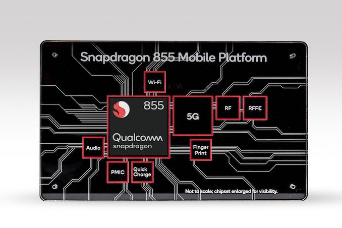
Given the mass success of Qualcomm’s Snapdragon 845 SoC in so many 2018 flagship smartphones, the next generation Snapdragon 855 has a lot to live up to. Today Qualcomm made their formal announcement about the 855 Mobile Platform, including most of the high-level specifications. We're looking into some of our question marks for a follow up piece, but here's the headline data.
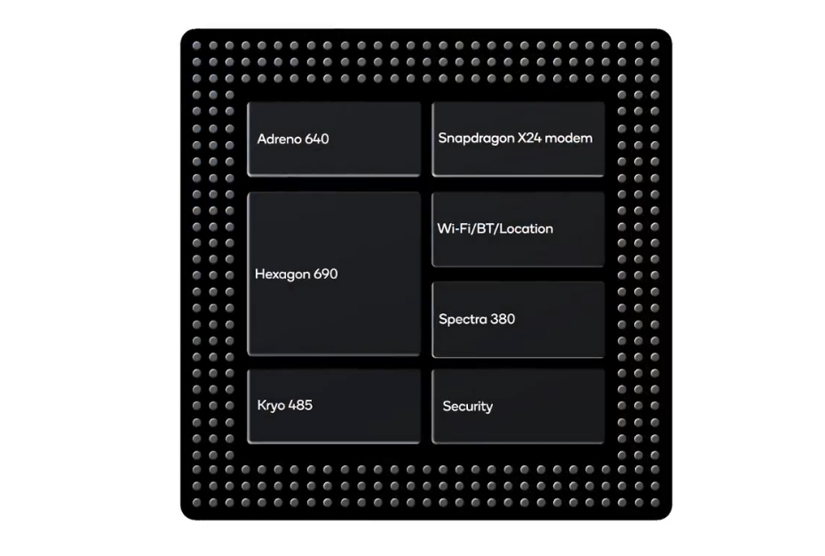
Qualcomm has listed a number of substantial improvements for the new generation SoC beyond what was announced yesterday. The key highlights include the Kryo 485 CPUs, the Adreno 640 graphics, the Hexagon 690 DSP, a two-gigabit X24 LTE modem, and improvements to the Spectra 380 ISP.
The Finer Details
Here’s our quick summary of day two at the Qualcomm Tech Summit.
| Qualcomm Snapdragon Flagship SoCs 2018-2019 | |||
| SoC | Snapdragon 855 | Snapdragon 845 | |
| CPU | 1x Kryo 485 Gold @ 2.84 GHz 3x Kryo 485 Gold @ 2.42 GHz 4x Kryo 485 Silver @ 1.80 GHz |
4x Kryo 385 Gold @ 2.80 GHz 4x Kryo 385 Silver @ 1.80 GHz |
|
| GPU | Adreno 640 @ ? MHz | Adreno 630 @ 710 MHz | |
| Memory | 4x 16-bit CH @ 2133 MHz LPDDR4x 34.1GB/s |
4x 16-bit CH @ 1866 MHz LPDDR4x 29.9GB/s |
|
| ISP/Camera | Dual 14-bit Spectra 380 ISP 1x 48MP or 2x 22 MP |
Dual 14-bit Spectra 280 ISP 1x 32MP or 2x 16 MP |
|
| Encode/ Decode |
2160p60 10-bit H.265 HDR10, HDR10+, HLG 720p480 |
2160p60 10-bit H.265 720p480 |
|
| Integrated Modem | Snapdragon X24 LTE (Category 20) DL = 2000Mbps 7x20MHz CA, 256-QAM, 4x4 UL = 316Mbps 3x20MHz CA, 256-QAM |
Snapdragon X20 LTE (Category 18/13) DL = 1200Mbps 5x20MHz CA, 256-QAM, 4x4 UL = 150Mbps 2x20MHz CA, 64-QAM |
|
| Mfc. Process | 7nm (N7) | 10nm LPP | |
At the heart of the new Snapdragon 855 lies Arm’s new Cortex A76 CPUs: We’ve covered the new microarchitecture extensively this year as we dove into the technical tidbits of the CPU in May, and more recently have been able to deep dive test the performance and power efficiency of the new IP inside HiSilicon’s new Kirin 980. The combination of the new Cortex A76 with the new 7nm manufacturing node made for great leaps in performance and power efficiency, something that bode very well for the new Snapdragon 855.
Qualcomm’s take on implementing the new Cortex A76 cores is quite a bit different to what we’ve seen from HiSilicon. Overall there’s still 4 Cortex A76 derived cores (Kryo 485 as Qualcomm markets them), alongside four Cortex A55 derived CPUs, also called Kryo 485. These are split into a 1+3+4 combination, offering a high 2.84 GHz single core frequency, a 2.42 GHz 'power cores' frequency, and a 1.82 GHz efficiency core frequency.
Qualcomm’s 2.84GHz clock is 9.2% higher than HiSilicon 2.6GHz frequency. A big question here is just how far Qualcomm has driven the core up on the power curve – I am expecting it to be less efficient than the Kirin 980 by some margin, how big that margin will be is something we won’t see until we get our hands on commercial devices.
In terms of performance, all that Qualcomm publishes is a claim of up to at 45% increase over the Snapdragon 845. As last year, it’s a bit of a mystery exactly what this figure represents, but the number pretty much falls in line exactly where the Kirin 980 performs in relation to the Snapdragon 845. The big question for the S855 is how the new generation system level cache will behave in terms of memory latency, as this will be among the biggest aspects differentiating Qualcomm’s new SoC.
Adreno 640 GPU
The Adreno 640 graphics will be the focus for Qualcomm’s gaming efforts. The company went to great lengths to detail that mobile gaming is on the rise, while other platforms for video games are either stagnating or in decline.
In terms of technical specifications, as is traditional with Qualcomm, we didn’t see much disclosures on the new GPU. What we did get promised are more conservative figures such as 20% increased performance. This increase is quite small compared to what we tend to usually see, especially given the fact that the Snapdragon 855 is able to take advantage of a major process node transition. It will be interesting to see if how it rlated to power.
While the performance gains remain a bit vague at time of writing, Qualcomm did disclose a lot in terms of new graphical features. Here we saw claims that the Adreno 640 graphics in the S855 will enable true HDR gaming, as well games built around Physically Based Rendering (more on that in a bit). The graphics pipeline will support 10-bit color depth and the Rec 2020 gamut to enable HDR, as well as enabling S855 devices to support the HDR10+ and Dolby Vision formats, which QC states is a world’s first. With the Adreno 640, along with the display IP, devices can support 120fps gaming as well as smooth 8K 360-degree video playback (resolving a major complaint about Snapdragon). Just don’t ask how much space those 8K 360-degree videos take up.
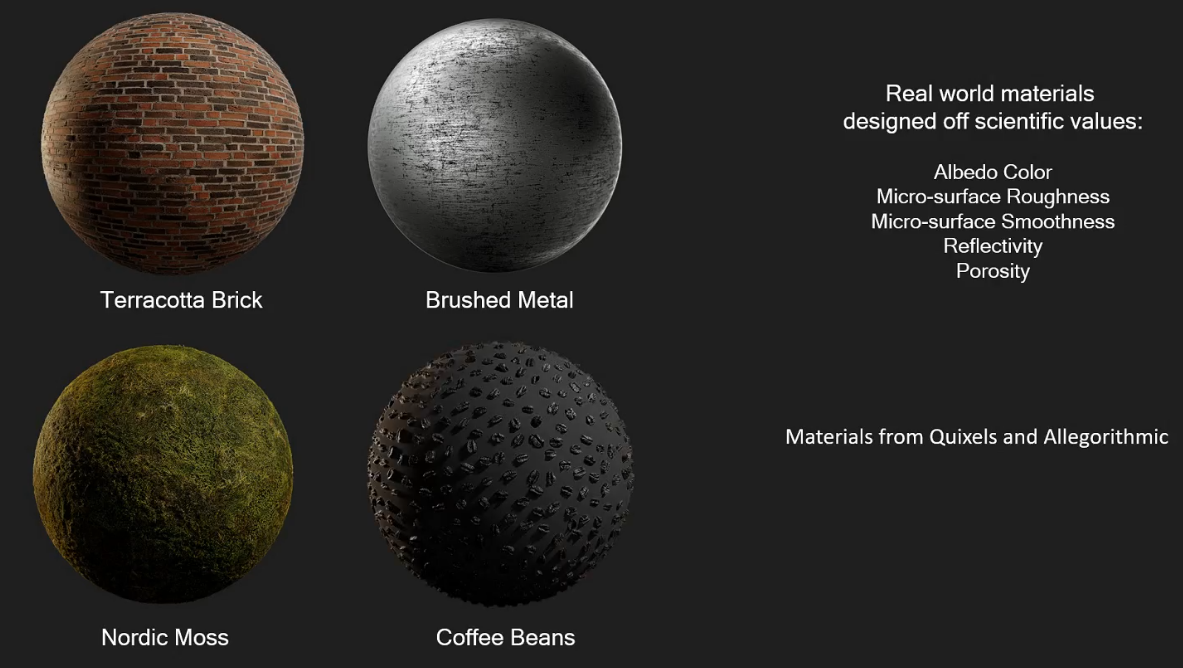
Qualcomm's support for Physically Based Rendering in graphics is an interesting topic, one we’ll go into detail in a different article, but the concept is not new (and technically shouldn't require any new hardware). The short version is that with this enabled, it will help add realism to gaming and augmented reality through more accurate lighting physics and material interactions. Qualcomm stated that through the Unity 4 engine, developers will be able to use real world materials designed from scientific values created by companies like Quixels and Allegorithmic that will make their environments more lifelike, such as the correct surface roughness / audio reflections or material-on-material interactions. This will also help with lighting and depth perception. More details to come.
Hexagon 690 DSP: The Heart of the AI Engine
The new Hexagon 690 is both an iteration on past generation units, as well as bringing a totally new aspect to the IP block. The new DSP block doubles up on the HVX vector pipelines compared to the Hexagon 680 and 685. As a reminder, the predecessor units contained four scalar units along with two 1024b vector processing units. The new Hexagon would thus contain four 1024b vector pipelines, doubling the processing power.
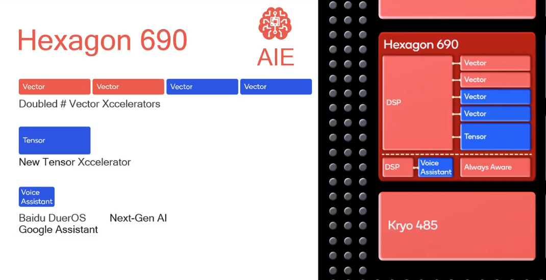
What is entirely new for the new Hexagon IP is the introduction of a new dedicated “tensor accelerator” unit that is seemingly tightly coupled within the larger block. This would most likely be a generally more simplistic MAC array resembling that of other neural network inferencing engines from other vendors. Effectively, this thus represents Qualcomm’s first generation dedicated ML inferencing engine, although Qualcomm does market it as a 4th generation “AI engine” (Previously this nomenclature referred to ML inferencing on CPU, GPU and DSP).
One of the interesting limitations Qualcomm had up to date is that the DSP wouldn’t have been able to process traditional DSP workloads alongside ML inferencing work – it’s still not clear at the time of writing if the new tensor unit can run concurrently alongside the vector units on two different workloads, but it would be a great win for the Snapdragon 855 if it would be able to.
Alongside the vector and tensor units is a new Voice Assistant AI module, designed to accelerate processing for common AI assistants – Qualcomm specifically states Baidu and Google in this case, although it’s unlikely to be exclusive to these two.
New Spectra 380 ISP: A Computer Vision Accelerator
Alongside the AI Engine, Qualcomm is pairing it with an upgraded Spectra 380 image signalling processor. It also gets a boost to its processing power with a tri-core Computer Vision (CV) ISP. This might seem a little odd – Computer Vision is a family of algorithms that we used to have before the latest advent of machine learning acceleration, so why is it here?
Computer Vision IP was big business, and by comparison to ML is computationally a lot lighter, and as such Qualcomm has deepened its ISP acceleration. With the CV-ISP, Qualcomm believes it can save 4x power (75%?) for image object classification, object segmentation, depth sensing (at 60 FPS), augmented reality body tracking, and image stabilisation.

With the new accelerator, Qualcomm states that rather than using the AI Engine for everything, the CV-ISP is preferred for these tasks due to the power saving. The company expects many of the features we normally take for granted in photography will now be available for video, such as 4K HDR at 60 FPS with both portrait mode enhancements and depth sensing for live bokeh. Power consumption for 4K HDR capture will be 30% lower than the Snapdragon 845.
Also on the cards is support for new generations of image files. Currently JPEG rules the roost in smartphone photography, however the new S855 will support ‘high efficiency image files’, or HEIF, which will offer a large number of new features over JPEG:
- Regular Images Up to 50% Smaller
- HDR Support for multiple color spaces
- Computer Vision data support
- RAW data
- Depth Map support
- Alpha Masking data
- Burst Photography data
- Animated Photography data
- HEVC Video data
The idea here is to enable new use cases for the photos that users take every day. Within the same HEIF, it can store a photo from every camera: a telephoto, a wide angle photo, and a super-wide angle photo for example. This allows of post processing such as bokeh adjustment, object segmentation, quality adjustments, and to a certain extent even basic 3D modelling.
Snapdragon 855 Connectivity
With day one being about Qualcomm’s approach to 5G, connectivity is going to be at the heart of the S855. Built into the chip is the Snapdragon X24 modem, which offers LTE Category 20 class download speeds good for up to 2 Gbps on supported devices and networks. The increased speeds is achieved by up to 7x carrier aggregation with 4x4 MIMO and 256QAM. On the upload side, the new SoC modem now also for the first time supports 256QAM, able to double the peak upload rate to up to 300Mbps with 3xCA.
In order to enable 5G, it’s not the actual SoC which delivers this, but an external Snapdragon modem in the form of the X50 is required. When combined with the S855, the platform will support both mmWave (>24 GHz) and sub-6 GHz 5G NR technologies.
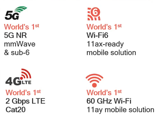
The Snapdragon 855 is a platform, and among one of the new platform capabilities is the support of the new WiFi 6 standard (802.11ax) as well as the new 60GHz “Wi-Gig” 802.11ay standard, enabled by an external WiFi combo chipset.
Next Year's Flagships
As mentioned at the top, the success of the S845 in 2018 flagships usually bodes well for the S855 in the next generation flagships. Today Qualcomm has various partners on site, including Samsung and OnePlus, that are available for 1-on-1 conversations. We're also expecting to pull more details about the Snapdragon 855 that immediately disclosed, so stay tuned for that.


7 Comments
View All Comments
tipoo - Wednesday, December 5, 2018 - link
It appears the one big-er 'Prime' core concept is paying dividends in ST performance, numbers floating around are a leap from 2400 in GB4 single core, to 3700, not bad for one generations jump.name99 - Wednesday, December 5, 2018 - link
Do we know EXACTLY what is going on with that Prime core? The way it's being sold is very strange.Suppose the pitch were 4 A76 (sorry, Kryo 485 Gold), maximum frequency of 2.84 GHz. No-one would be upset if that means when ONE core is running, it hits 2.84 GHz, and this drops when two or more are running. Everybody does that -- other mobile, Apple, Intel, etc.
So what's different? The obvious answer is that only ONE of the cores can hit 2.84GHz. But even that raises a whole bunch of questions like
- why draw attention to this? It's a weakness, not a strength; but it can be hidden by just having the OS always place the single thread on the Prime core, not on just any core.
- is this something detected by testing? ie design to 2.84 GHz, then choose whichever of the 4 runs that at lowest power? There might actually be some good sense to that (generically, rank ALL cores by power burned, and have the OS use that in scheduling) but again why make this public?
- or is this core deliberately different? Like some part of it (I assume not much, just a few critical paths) uses high performance rather than low power transistors? Is that effort worth an extra 15% performance (hopefully at not too much energy cost)? I'd have to see the actual performance/power tradeoff, but it IS (IMHO) an intriguing idea.
On Twitter I've mulled over the idea of Apple offering a faster than Vortex core (but higher power) with the AX SoCs offering something like 1V+ & 3V & 4T cores, which is what QC appear to be doing here. What I had in mind was a more aggressively designed super-core, but even a tweaked+recompiled version of a Vortex core (ie, like I said, upgrade just the transistors in the critical paths) does the job and 15% is 15% --- that's about a half-generation performance boost which ain't nothing.
So, yeah, IMHO can the whining! There are some very nice ideas here.
The beefed up DSP, for example, remains a nice feature and I keep wondering if that's another block of silicon that Apple will eventually (these things take time!) drop onto its SoCs. Certainly the sorts of things they are offering with this tech (like photography feature, available to video) are good ideas, and I wonder if Apple will be offering them next year.
tipoo - Wednesday, December 5, 2018 - link
The Prime core has twice the L2 cache for onehttps://www.anandtech.com/show/13680/snapdragon-85...
It's possibly also the best binned for higher clocks, like Intel is starting to do now? Not sure. But yeah, the extra cache and highest turbo alone still make for a pretty interesting ST performance bump.
Frenetic Pony - Wednesday, December 5, 2018 - link
What a bunch of disappointing nonsense.Vague handwavy specs to outright lies to... I don't even know what some of this press conference was. "Our hardware supports PBR!" is the most nonsensical statement I've ever seen. It's like congratulating yourself on releasing a car that can fit things inside it.
Who the hell was this conference for? What was the point? I think tech companies that make internal, non consumer facing components have gone batshit for weird PR conferences like this. They tell tech people nothing true or relevant. They tell consumers nothing they care about. So who are they selling too? These things seem to exist only so PR people at the company can justify having a job.
Meteor2 - Wednesday, December 5, 2018 - link
Did you get out of bed on the wrong side this morning?WasHopingForAnHonestReview - Wednesday, December 5, 2018 - link
Next he complain how it's Trump's fault.BurntMyBacon - Thursday, December 6, 2018 - link
@Frenetic Pony: "These things seem to exist only so PR people at the company can justify having a job."I believe you now understand fully half of why marketing employees do the things they do.