IBM to use Samsung 7nm EUV for Next-Gen POWER and z CPUs
by Anton Shilov on December 21, 2018 11:30 AM EST- Posted in
- CPUs
- IBM
- POWER
- Semiconductors
- EUV
- 7nm
- Samsung Foundry
- IBM Z
IBM has announced it has signed an agreement with Samsung Foundry to produce its next-generation processors. This includes processors for IBM Power Systems, IBM z, and LinuxONE systems, all using Samsung’s 7 nm fabrication process that uses extreme ultraviolet lithography (EUVL). The decision comes as no surprise as GlobalFoundries, IBM’s manufacturing partner for CPUs, decided to abandon development of 7 nm and more advanced technologies. IBM and Globalfroundies manufacturing agreement, whereby fabs, IP, and $$ were given to GlobalFoundries to make IBM's CPUs, ends this month.
IBM and Samsung have collaborated for 15 years researching and developing various semiconductor production materials and technologies as part of IBM’s Research Alliance. Considering the fact that Samsung’s and GlobalFoundries’ fabrication processes rely on R&D conducted internally and as part of IBM’s Research Alliance, IBM developers know what to expect from these technologies. IBM said that under the current agreement, the two companies will expand and extend the strategic partnership, but did not elaborate whether this means development of a custom version of Samsung’s 7LPP manufacturing process for IBM. At present, the companies call the tech to be used for IBM’s chips as “7 nm EUV”.
IBM has traditionally used custom manufacturing processes to build its IBM POWER processors for servers and IBM z CPUs for mission-critical mainframes. IBM’s chips combine a high core count and complexity with very high frequencies, which is why the company required highly-custom process technologies that relied on SOI wafers, featured an increased amount of metal layers, a reduced transistor density, and other adjustments. Typically, technologies fine-tuned for IBM CPUs by IBM Microelectronics and then GlobalFoundries were only used for these products (partly because of IP and partly because of costs).
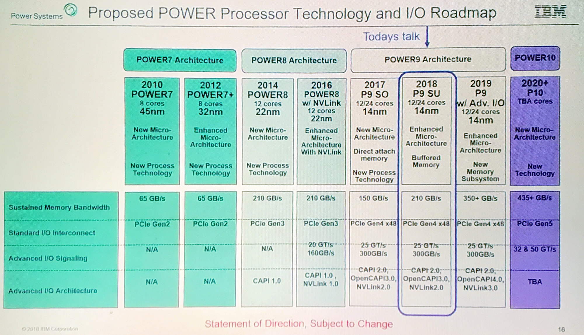
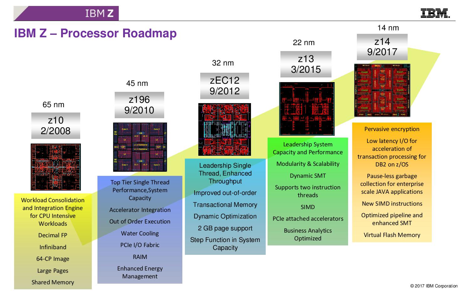
The two companies also did not disclose what exactly Samsung Foundry will produce for IBM. Based on IBM’s current roadmap for POWER processors, its 2019 CPUs will be made by GlobalFoundries using a custom 14 nm fabrication process. Meanwhile, the company’s next-gen POWER10 products set to hit the market in 2020 or later will allegedly use a different manufacturing tech. Meanwhile, IBM’s next-gen z15 processors for IBM Z mainframes, which are not introduced on a per-annum cadence, will most likely be fabbed by Samsung.
Samsung Foundry recently started to use its 7LPP manufacturing tech for high-volume production of undisclosed chips. This fabrication process uses EUVL tools for select layers only in a bid to reduce cycle times.
Related Reading
- GlobalFoundries Weds FinFET and SOI in 14HP Process Tech for IBM z14 CPUs
- Hot Chips: IBM's Next Generation z14 CPU Mainframe Live Blog (5pm PT, 12am UTC)
- Assessing IBM's POWER8, Part 2: Server Applications on OpenPOWER
- GlobalFoundries Stops All 7nm Development: Opts To Focus on Specialized Processes
- Samsung Starts Mass Production of Chips Using Its 7nm EUV Process Tech
Sources: IBM, Samsung


24 Comments
View All Comments
Kevin G - Friday, December 21, 2018 - link
This is a big change for Samsung as they'll have to have their fabs capable of handling >600 mm^2 designs and >5 Ghz frequencies. They did some high performance stuff like this in the past (DEC Alpha) but that is decades ago on 250 nm process. IBM could go the chiplet route (and they kind of do already on zSeries with the system controllers being on package with multiple CPU dies) to avoid the high size criteria but there is still the frequency aspect.POWER10 could likely move to Samsung with little issue but zSeries is used in some critical US government facilities and moving manufacturing overseas may meet some resistance.
CoreDuo - Friday, December 21, 2018 - link
Samsung has a huge fab in Austin, TX.jeremyshaw - Friday, December 21, 2018 - link
14nm, iirc. The 10 and 7nm stuff is in Korea.On a tangent, wasn't Nvidia's first plan for this gen Ampere @ Samsung 10nm? AFAIK, that fell through and Turing was quickly spun up on familiar TSMC 12FFN to fill in the gap. Turing showed up really late on the roadmaps, which is probably where that rumor comes from.
IBM also demoed 7nm EUV first with Samsung, several years ago. IBM & Nvidia probably have a vested interest (more than OpenPOWER) in getting large ASIC working on Samsung processes, since the "only option" is TSMC (Intel tends to shy away from making larger dies).
CoreDuo - Friday, December 21, 2018 - link
Doesn't mean that it has to stay that way. If push comes to shove, they could retrofit or expand it.FullmetalTitan - Saturday, December 22, 2018 - link
With 7nm processes widely expected to be a long term node for the industry, the way 14nm has been, I wouldn't be surprised if Samsung does announce a new FAB somewhere within the next 2 years. May not be 7nm, could be part of their 5nm ramp up as capacity shuffling happensrocketbuddha - Friday, December 21, 2018 - link
Well. There goes Global F(l)oundries down to the bin. Let us see how they spin this one. So after AMD spun off GF in 2005, there was only 1 node they made somewhat reasonably commerically viable for a small period 28nm bulk.They basically swallowed Chartered, IBM Micro and still had all the FD-SOI nodes in the world and still cannot do any s**t out of it.
Clever IBM, hive off its Fabs to the universal graveyard and now move to some other competitor. With GF now deciding that 12nm is their current best 1-1.5 generations behind others, what clients will they have for their supposedly top FinFET and FD-SOI nodes??
LOL!
jeremyshaw - Friday, December 21, 2018 - link
IBM had to pay ~$1.5B USD to get GF to take over it's fabs. AFAIK, IBM's fabs were run at quite a loss. Why GF thought it was a good idea to take on IBMs fabs, remains a mystery.ZeDestructor - Sunday, December 23, 2018 - link
The answer to that is obvious: the figured increased capacity would get them more contracts and revenue. Unfortunately for em, it didn't pan out.ZolaIII - Friday, December 21, 2018 - link
Well as much as I can recall the 14nm costume should be a 14nm FinFET structure with SOI wafer, if the EUV turns to be cost cutting enough for additional benefits that it brings the migration will be swift and rather sooner than later. The 7nm EUV Samsung presented so far is based on High Density Lib, the road map also shows "5nm EUV" which will actually be a same o 7nm with Ultra High Density lib, but I doubt IBM will use that (because performance goals they have). Judging by announcements this should be a late 2019 shirt if IBM is serious & wants to gain some momentum.The_Assimilator - Friday, December 21, 2018 - link
So some bright spark exec at IBM decided that they'll cut costs by going fabless and letting GloFo pay for fabbing R&D.. then GloFo turns around and says "BTW we don't feel like paying for R&D anymore"... and now IBM has had to go, hat in hand, to Samsung to ask to use their fab. I wonder how much that's costing IBM... I wonder if they are prepared for the low-quality shitfest that is Samsung's power-leaking chips?