TSMC’s 5nm EUV Making Progress: PDK, DRM, EDA Tools, 3rd Party IP Ready
by Anton Shilov on April 5, 2019 12:00 PM EST- Posted in
- Semiconductors
- EUV
- TSMC
- 5nm
- CLN5
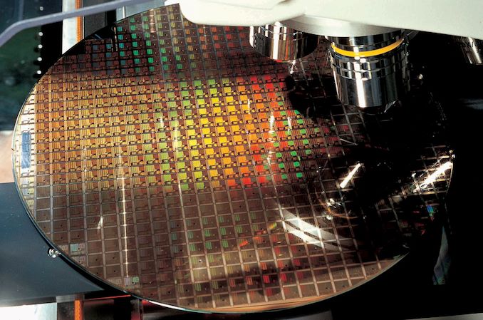
TSMC this week said that it has completed development of tools required for design of SoCs that are made using its 5 nm (CLN5FF, N5) fabrication technology. The company indicated that some of its alpha customers (which use pre-production tools and custom designs) had already started risk production of their chips using its N5 manufacturing process, which essentially means that the technology is on-track for high-volume manufacturing (HVM) in 2020.
TSMC’s N5 is the company’s 2nd generation fabrication technology that uses both deep ultraviolet (DUV) as well as extreme ultraviolet (EUV) lithography. The process can use EUVL on up to 14 layers (a tangible progress from N7+, which uses EUVL on four non-critical layers) to enable significant improvements in terms of density. TSMC says that when compared to N7 (1st Gen 7 nm, DUV-only), N5 technology will allow chip developers to shrink die area of their designs by ~45%, making transistor density ~1.8x higher. It will also increase frequency by 15% (at the same complexity and power) or reduce power consumption by 20% power reduction (at the same frequency and complexity).
| Advertised PPA Improvements of New Process Technologies Data announced by companies during conference calls, press briefings and in press releases |
||||||||
| TSMC | ||||||||
| 16FF+ vs 20SOC |
10FF vs 16FF+ |
7FF vs 16FF+ |
7FF vs 10FF |
7FF+ vs 7FF |
5FF vs 7FF |
|||
| Power | 60% | 40% | 60% | <40% | 10% | 20% | ||
| Performance | 40% | 20% | 30% | ? | same (?) | 15% | ||
| Area Reduction | none | >50% | 70% | >37% | ~17% | 45% | ||
TSMC finished development of N5 some time ago and its alpha customers with access to pre-production tools are already risk producing chips using the technology. Meanwhile, TSMC has finalized its 5 nm design rule manual (DRM), process design kits (PDKs), and SPICE (simulation program with integrated circuit emphasis) model for those clients who prefer to work with a stable version of design infrastructure.
Besides TSMC’s tools, chip developers can also use a comprehensive set of EDA (electronic design automation) tools from ANSYS, Cadence, Mentor Graphics, and Synopsys. TSMC says that EDA programs from the said companies fully support N5 DRM to ensure necessary accuracy, routability for optimized power, and other aspects of the technology. Obviously, all the tools have been certified by the contract maker of semiconductors.
Finally, TSMC and its partners have also developeda comprehensive N5 IP portfolio that is currently focused primarily on HPC and mobile SoCs. TSMC’s Foundation IP includes high-density and high-performance sets of standard cell libraries and memory compilers. Meanwhile, the company’s partners offer a variety of IP cores for N5 SoCs, including DDR, LPDDR, MIPI, PCIe, and USB PHYs.
“TSMC’s 5-nanometer technology offers our customers the industry’s most advanced logic process to address the exponentially growing demand for computing power driven by AI and 5G,” said Cliff Hou, Vice President of Research & Development/Technology Development at TSMC. “5-nanometer technology requires deeper design-technology co-optimization. Therefore, we collaborate seamlessly with our ecosystem partners to ensure we deliver silicon-validated IP blocks and EDA tools ready for customer use. As always, we are committed to helping customers achieve first-time silicon success and faster time-to-market.”
All the tools required for development of chips to be made using N5 fabrication technology are available from TSMC and its partners right now.
Related Reading
- TSMC: First 7nm EUV Chips Taped Out, 5nm Risk Production in Q2 2019
- TSMC Details 5 nm Process Tech: Aggressive Scaling, But Thin Power and Performance Gains
- TSMC Starts to Build Fab 18: 5 nm, Volume Production in Early 2020
Source: TSMC


31 Comments
View All Comments
Opencg - Friday, April 5, 2019 - link
wow those are sizeable increased to speed or power. i wonder how expensive it will be with the euv layers.Gondalf - Friday, April 5, 2019 - link
I don't think so, looking at the chart 5nm is only less than an half node vs 7nm and a little more than nothing over 7nm+. Likely many will stay on 7nm+ or 7nm, both cheaper and with similar performance.Not impressed at all from this new node, thinked for few phone SOCs only unfortunately.
At 5nm we need of new transistors to have real advantages.
Cellar Door - Friday, April 5, 2019 - link
You clearly are not comprehending the die size reduction - hence the ability for higher yields. This and power consumption will be strong enough drivers for this process to take off.JoeyJoJo123 - Friday, April 5, 2019 - link
>the ability for higher yieldsThat only happens after the process hits a point of maturity and is refined such that the expenses of manufacturing the wafer are suitably compensated by the inherent value gained by the chips on the wafer. The initial complexity of the shrink leaves most chips imperfect and inherently unusable after strict QA standards mark which chips are acceptable and which won't work.
It took a really long time for 7nm yields to be good enough for public consumption, and we're still waiting for most of those 7nm products to hit the market. Intel's _still_ having issues with 10nm node yields.
While 5nm wafers can yield "more chips" per unit wafer, they also cost more than 7, 10, or 14nm wafers. You need to basically hit a point to where manufacturing of 5nm wafers is more profitable than continuing to manufacture the lower density wafers which are very refined processes with very good yields. 5nm processes will _eventually_ hit good enough yields to replace those other process nodes, but that's going to take a long time. The article only details that TSMC is seeing some initial promise with their 5nm process.
sgeocla - Friday, April 5, 2019 - link
While NVidia GPUs or Apple big chips (iPad & possible laptop chips) are going to take a while to be profitable, AMD Zen3 chiplets on 5nm (45nm2) for higher performance/frequency EPYCs are going to be extremely profitable (a.k.a. "cheeplets").Since the chiplets architecture allows AMD to speed up core & io design and validation significantly we could probably see this by end of 2020 coupled with DDR5 and PCIe 5.0.
Antony Newman - Sunday, April 7, 2019 - link
For large SOCs - reducing their area by 1.8 times, on the same process, will improve yields (especially if the current yield is low).When ASML move to High Numerical Aperture EUV System - many of the error deviations will reduce over their existing system (although LERoughness could be the upper limit on yields).
AJ
Zingam - Sunday, April 7, 2019 - link
At that speed of progress you'll be browsing the Internet on a googol numbered Chrome version on a subPlanck constant process!:)
Long live marketing blurbs!
ksec - Friday, April 5, 2019 - link
There are no more "new node" since 16nm from TSMC, every node since than has been an iteration of previous node. Trying to improve things step by step rather than the old "Intel" way of full new node. It is the same with 5nm. Once 5nm matures those 7nm customers will move to it.Not to mention you are getting a new quite a bit of area reduction and performance in only 12 months time.
ZolaIII - Saturday, April 6, 2019 - link
The 10 nm whose a full node but it didn't lived long enough nor whose adopted much so in industry it whose considered as half node, 7 nm is a full node and so is (at least based on press material) 5 nm. Real half node's are 14 nm, 12 nm based on 16 nm one. The new structure Gate All Around is being worked on and EUV will see it's full utilisation approximately at the same time, FF reached it's expected full potential with 7 (10 really) nm, 5 nm is stretch beyond expected.evernessince - Monday, July 15, 2019 - link
"Intel way"? Oh you mean like actually giving results instead of 5 years of delay.