The Snapdragon 865 Performance Preview: Setting the Stage for Flagship Android 2020
by Andrei Frumusanu on December 16, 2019 7:30 AM EST- Posted in
- Mobile
- Qualcomm
- Smartphones
- 5G
- Cortex A77
- Snapdragon 865

Earlier this month we had the pleasure to attend Qualcomm’s Maui launch event of the new Snapdragon 865 and 765 mobile platforms. The new chipsets promise to bring a lot of new upgrades in terms of performance and features, and undoubtedly will be the silicon upon which the vast majority of 2020 flagship devices will base their designs on. We’ve covered the new improvements and changes of the new chipset in our dedicated launch article, so be sure to read that piece if you’re not yet familiar with the Snapdragon 865.
As has seemingly become a tradition with Qualcomm, following the launch event we’ve been given the opportunity to have some hands-on time with the company’s reference devices, and had the chance to run the phones through our benchmark suite. The QRD865 is a reference phone made by Qualcomm and integrates the new flagship chip. The device offers insight into what we should be expecting from commercial devices in 2020, and today’s piece particularly focuses on the performance improvements of the new generation.
- Qualcomm Announces Snapdragon 865 and 765(G): 5G For All in 2020, All The Details
- Qualcomm Windows on Snapdragon: New 7c & 8c SoCs for sub-$800 Laptops
- Quick Bytes: Qualcomm’s Dynamic Spectrum Sharing Demo with 5G and 4G
- Quick Bytes: Qualcomm’s Prediction of 1.4 Billion 5G Smartphones by 2022
- Qualcomm Snapdragon Tech Summit Live Blog: Day One
- Qualcomm Snapdragon Tech Summit Live Blog Day Two: All About Mobile
- Qualcomm Snapdragon Tech Summit Day 3 Live Blog: ACPC and XR
A quick recap of the Snapdragon 865 if you haven’t read the more thorough examination of the changes:
| Qualcomm Snapdragon Flagship SoCs 2019-2020 | |||
| SoC |
Snapdragon 865 |
Snapdragon 855 | |
| CPU | 1x Cortex A77 @ 2.84GHz 1x512KB pL2 3x Cortex A77 @ 2.42GHz 3x256KB pL2 4x Cortex A55 @ 1.80GHz 4x128KB pL2 4MB sL3 @ ?MHz |
1x Kryo 485 Gold (A76 derivative) @ 2.84GHz 1x512KB pL2 3x Kryo 485 Gold (A76 derivative) @ 2.42GHz 3x256KB pL2 4x Kryo 485 Silver (A55 derivative) @ 1.80GHz 4x128KB pL2 2MB sL3 @ 1612MHz |
|
| GPU | Adreno 650 @ 587 MHz +25% perf +50% ALUs +50% pixel/clock +0% texels/clock |
Adreno 640 @ 585 MHz |
|
| DSP / NPU | Hexagon 698 15 TOPS AI (Total CPU+GPU+HVX+Tensor) |
Hexagon 690 7 TOPS AI (Total CPU+GPU+HVX+Tensor) |
|
| Memory Controller |
4x 16-bit CH @ 2133MHz LPDDR4X / 33.4GB/s or @ 2750MHz LPDDR5 / 44.0GB/s 3MB system level cache |
4x 16-bit CH @ 1866MHz LPDDR4X 29.9GB/s 3MB system level cache |
|
| ISP/Camera | Dual 14-bit Spectra 480 ISP 1x 200MP 64MP ZSL or 2x 25MP ZSL 4K video & 64MP burst capture |
Dual 14-bit Spectra 380 ISP 1x 192MP 1x 48MP ZSL or 2x 22MP ZSL |
|
| Encode/ Decode |
8K30 / 4K120 10-bit H.265 Dolby Vision, HDR10+, HDR10, HLG 720p960 infinite recording |
4K60 10-bit H.265 HDR10, HDR10+, HLG 720p480 |
|
| Integrated Modem | none (Paired with external X55 only) (LTE Category 24/22) DL = 2500 Mbps 7x20MHz CA, 1024-QAM UL = 316 Mbps 3x20MHz CA, 256-QAM (5G NR Sub-6 + mmWave) DL = 7000 Mbps UL = 3000 Mbps |
Snapdragon X24 LTE (Category 20) DL = 2000Mbps 7x20MHz CA, 256-QAM, 4x4 UL = 316Mbps 3x20MHz CA, 256-QAM |
|
| Mfc. Process | TSMC 7nm (N7P) |
TSMC 7nm (N7) |
|
The Snapdragon 865 is a successor to the Snapdragon 855 last year, and thus represents Qualcomm’s latest flagship chipset offering the newest IP and technologies. On the CPU side, Qualcomm has integrated Arm’s newest Cortex-A77 CPU cores, replacing the A76-based IP from last year. This year Qualcomm has decided against requesting any microarchitectural changes to the IP, so unlike the semi-custom Kryo 485 / A76-based CPUs which had some differing aspects to the design, the new A77 in the Snapdragon 865 represents the default IP configuration that Arm offers.
Clock frequencies and core cache configurations haven’t changed this year – there’s still a single “Prime” A77 CPU core with 512KB cache running at a higher 2.84GHz and three “Performance” or “Gold” cores with reduced 256KB caches at a lower 2.42GHz. The four little cores remain A55s, and also the same cache configuration as well as the 1.8GHz clock. The L3 cache of the CPU cluster has been doubled from 2 to 4MB. In general, Qualcomm’s advertised 25% performance uplift on the CPU side solely comes from the IPC increases of the new A77 cores.
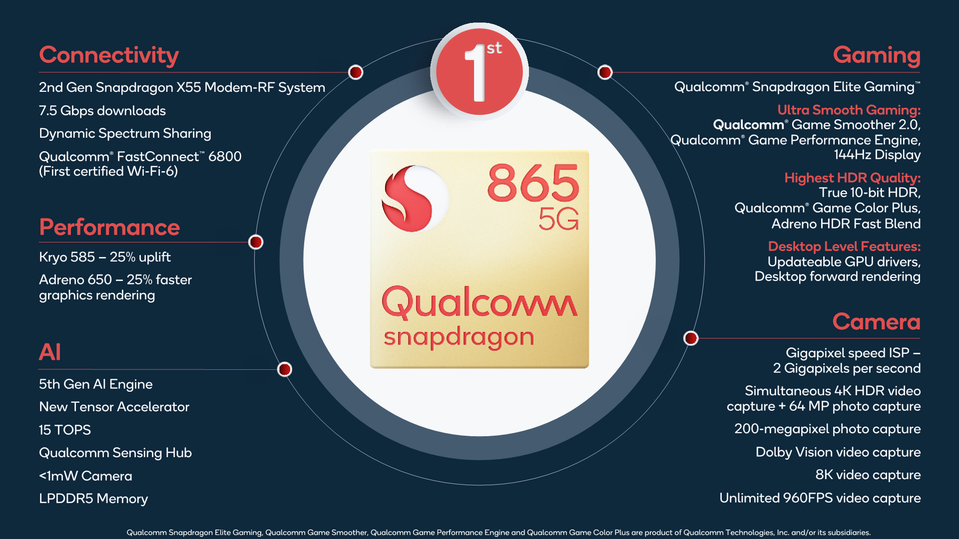
The GPU this year features an updates Adreno 650 design which increases ALU and pixel rendering units by 50%. The end-result in terms of performance is a promised 25% upgrade – it’s likely that the company is running the new block at a lower frequency than what we’ve seen on the Snapdragon 855, although we won’t be able to confirm this until we have access to commercial devices early next year.
A big performance upgrade on the new chip is the quadrupling of the processing power of the new Tensor cores in the Hexagon 698. Qualcomm advertises 15 TOPS throughput for all computing blocks on the SoC and we estimate that the new Tensor cores roughly represent 10 TOPS out of that figure.
In general, the Snapdragon 865 promises to be a very versatile chip and comes with a lot of new improvements – particularly 5G connectivity and new camera capabilities are promised to be the key features of the new SoC. Today’s focus lies solely on the performance of the chip, so let’s move on to our first test results and analysis.
New Memory Controllers & LPDDR5: A Big Improvement
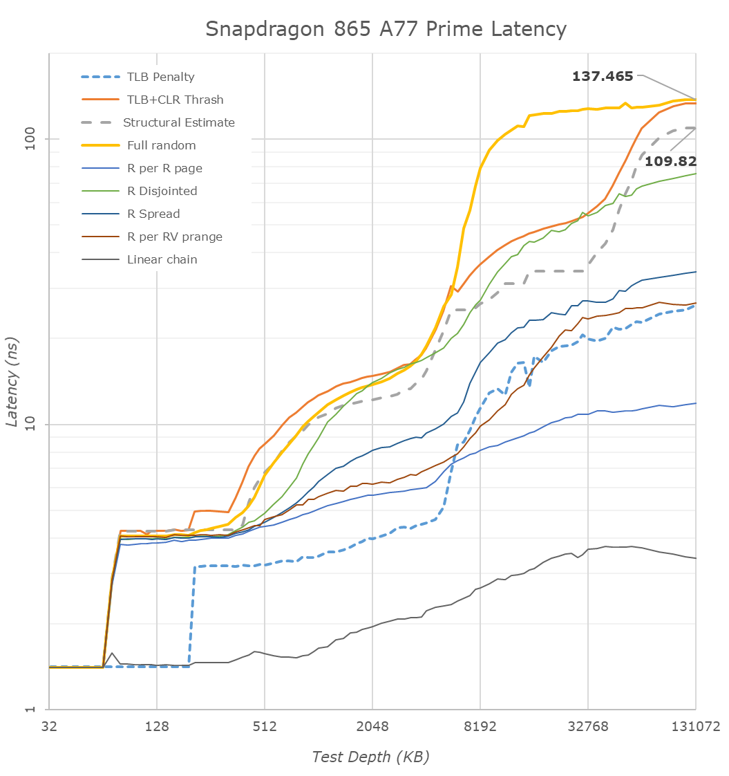
One of the larger changes in the SoC this generation was the integration of a new hybrid LPDDR5 and LPDDR4X memory controller. On the QRD865 device we’ve tested the chip was naturally equipped with the new LP5 standard. Qualcomm was actually downplaying the importance of LP5 itself: the new standard does bring higher memory speeds providing better bandwidth, however latency should be the same, and power efficiency benefits, while there, shouldn’t be overplayed. Nevertheless, Qualcomm did claim they focused more on improving their memory controllers, and this year we’re finally seeing the new chip address some of the weaknesses exhibited by the past two generations; memory latency.
We had criticised Qualcomm’s Snapdragon 845 and 855 for having quite bad memory latency – ever since the company had introduced their system level cache architecture to the designs, this aspect of the memory subsystem had seen some rather mediocre characteristics. There’s been a lot of arguments in regards to how much this actually affected performance, with Qualcomm themselves naturally downplaying the differences. Arm generally notes a 1% performance difference for each 5ns of latency to DRAM, if the differences are big, it can sum up to a noticeable difference.
( )
Looking at the new Snapdragon 865, the first thing that pops up when comparing the two latency charts is the doubled L3 cache of the new chip. It’s to be noted that it does look that there’s still some sort of logical partitioning going on and 512KB of the cache may be dedicated to the little cores, as random-access latencies start going up at 1.5MB for the S855 and 3.5MB for the S865.
Further down in the deeper memory regions, we’re seeing some very big changes in latency. Qualcomm has been able to shave off around 35ns in the full random-access test, and we’re estimating that the structural latency of the chip now falls in at ~109ns – a 20ns improvements over its predecessor. While it’s a very good improvements in itself, it’s still a slightly behind the designs of HiSilicon, Apple and Samsung. So, while Qualcomm still is the last of the bunch in regards to its memory subsystem, it’s no longer trailing behind by such a large margin. Keep in mind the results of the Kirin 990 here as we go into more detailed analysis of memory-intensive workloads in SPEC on the next page.
Furthermore, what’s very interesting about Qualcomm’s results in the DRAM region is the behaviour of the TLB+CLR Trash test. This test is always hitting the same cache-line within a page across different, forcing a cache line replacement. The oddity here is that the Snapdragon 865 here behaves very differently to the 855, with the results showcasing a separate “step” in the results between 4MB and ~32MB. This result is more of an artefact of the test only hitting a single cache line per page rather than the chip actually having some sort of 32MB hidden cache. My theory is that Qualcomm has done some sort of optimisation to the cache-line replacement policy at the memory controller level, and instead the test hitting DRAM, it’s actually residing at on the SLC cache. It’s a very interesting result and so far, it’s the first and only chipset to exhibit such behaviour. If it’s indeed the SLC, the latency would fall in at around 25-35ns, with the non-uniform latency likely being a result of the four cache slices dedicated to the four memory controllers.
Overall, it looks like Qualcomm has made rather big changes to the memory subsystem this year, and we’re looking forward to see the impact on performance.


178 Comments
View All Comments
UglyFrank - Monday, December 16, 2019 - link
I imagine the Tab S7 will have this.Meanwhile the iPad Pro 2020 will most likely have more than double the GPU power.
Kishoreshack - Monday, December 16, 2019 - link
That's not how it works broUglyFrank - Monday, December 16, 2019 - link
It is. The A12X has more than double the S855's GPU performance and we can expect ~ 20% increase in GPU performance (A12X to A13X) as the A12 to A13 had a similar increase.generalako - Monday, December 16, 2019 - link
Ok, but then again the SD875 (or whatever it will be called) is expected to be on a new architecture after 3 generation, which generally means 50%+ jump just there. With the transition over to 5nm, you can expect even more performance from that. That would, after all, be the most fair comparison to the A14 (or A14X) on 5nm later this year, due to process node comparisons. Same with CPUs (don't forget, the A77 in the SD865 was released in the summer before by ARM, and even presented in the SD865 in December).close - Tuesday, December 17, 2019 - link
Over the past few years Apple has been doing a consistently better job than Qualcomm regardless of process node. Probably they can afford to since they are in full control of the whole technology stack, including the software which means they can squeeze additional performance and efficiency like that. But this doesn't change the fact that year after year A-chips are better than their counterparts.tuxRoller - Wednesday, December 18, 2019 - link
I'm not sure that apple is much, if at all, more optimized than the Android bsps. If you're aware of proof to the contrary I'd be interested in reading it.michael2k - Wednesday, December 18, 2019 - link
It doesn’t mean optimized the way you envision it. It means more tailored to the design, since Apple has a fixed number of systems it has to support. There are three ways to see it: how many years does Apple push iOS updates? That is a function of performance as well, as as the OS.Another way to see it is knowing that Apple ships iPhones with much less RAM, meaning their OS and apps have to be designed to use less RAM too.
Likewise their iPhone usually ships with smaller batteries; by designing the OS, SoC, and RAM synergistically they can use a smaller battery too. RAM happens to use energy even when idle, so less RAM does translate to lower energy usage.
michael2k - Tuesday, December 17, 2019 - link
Yeah, but anything Qualcomm does to boost performance, Apple will be doing too.The 865 is going to compete with the A14 in 2020, and the 875 will compete with the A15 in 2021. So if we expect the A14 to boost perf by 15% and the A14X to boost perf by 40%, and the A15 to boost perf again by 10% and A15X to boost perf again by 25%, you'll see:
855 = 1.00
865 = 1.25
875 = 1.50
A13 = 1
A13X = 1.4
A14 = 1.15
A14X = 1.96
A15 = 1.26
A15X = 2.45
Technically Qualcomm has more room to improve when you compare transistor budgets: the A13 is approximately 8.5b transistors, the A12 7b transistors.
In comparison, the 855 only had 6b transistors, per Qualcomm itself:
https://www.qualcomm.com/media/documents/files/sna...
id4andrei - Tuesday, December 17, 2019 - link
The 865 competes with A13 not with the future A14. Apple sets the cadence in the SoC space and have done so since breaking rank with sheer performance and transition to a 64bit arch.generalako - Tuesday, December 17, 2019 - link
This is just misrepresentative. The past two generations ARM's architecture has been closing the gap to Apple. It closed the gap by around 30% in IPC with A76, and doing so by around 15% in IPC with A77 (A77 had 27% IPC gain vs. A13's 12% IPC gain). The gap has been getting smaller, and hopefully it will continue. But the fact is still that it's closing for the performance cores.Also, you're comparisons are way off. The SD855 was comparable to the A12, just as the SD865 is to the A13, and so on and so forth. This with process node and the actual release date of the Cortex Core in mind.