AMD Ryzen Mobile 4000: Measuring Renoir’s Die Size
by Dr. Ian Cutress on January 14, 2020 9:00 AM EST- Posted in
- CPUs
- AMD
- Trade Shows
- Ryzen Mobile
- Renoir
- CES 2020
- Ryzen 4000
I’m pretty sure that the next time I go to a trade show where new silicon is being announced, the next tool I need in my backpack is a set of calipers in order to measure the die size. While die size doesn’t in of itself mean much as a number on its own, it is the end result of lots of hard work, focused co-design between silicon engineers and the semiconductor fabs, and ultimately there’s a fine balance between features, die size, performance, power, and at the end of the day, cost. With AMD showcasing the first x86-based 8-core CPU to move into the 15 W power envelope, finding out the die size is one of the elements of our investigation into how AMD has created its new Renoir / Ryzen Mobile 4000 product.
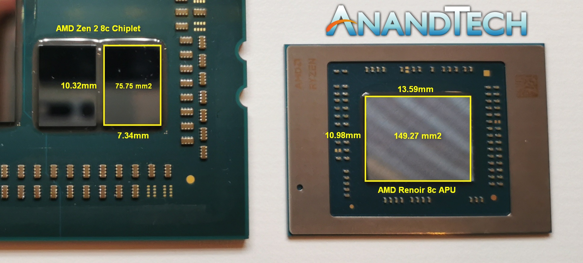
When I first saw the silicon, I wasn’t able to take pictures. Instead, I had to guess the size by manually placing it next to a 8-core Zen 2 chiplet from AMD’s monster 64-core Threadripper 3990X. We’ve known the die size for a while now, at 10.32 x 7.34 mm, or 75.75 mm2. My guess at the time that the new Renoir APU was almost exactly double the Zen 2 chiplet, and I mean it was scary how close to double the size it was. At the time of the announcement of Ryzen Mobile 4000, I had stated in our article that I estimated 150 mm2 for the die size. Turns out, I wasn’t too far wrong.
This image is not to scale.
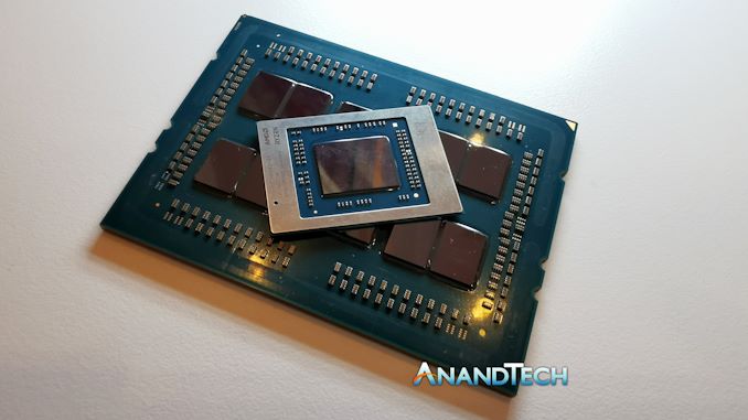
Later at CES, I went up to the AMD booth and this time they were more than happy for me to take photographs of the new silicon. The 3990X was also there, so I could place the two side by side and get a reasonable reference photograph on which to do calculations. This is the point of the event where I should have remembered to bring calipers! Taking photographs of chips is actually quite hard, making sure you get them lined up perfectly to get the same perspective, but also having enough light to get clear defined silicon edges.
In our picture, the Renoir chiplet you may notice is very slightly angled to the camera, which we’ve compensated for in our measurements.
With that in mind, here are our numbers.
The Zen 2 chiplet on the left, measures 10.32 mm by 7.34 mm, which is a ratio of 1.406 to 1.
In our image, the chiplet measured 265 pixels by 189 pixels, which is a ratio of 1.402 to 1.
In our image, the Renoir SoC measured 282 pixels by 350 pixels, which is a ratio of 0.806 to 1.
If we take the corresponding pixel dimensions, that gives us 10.98 mm by 13.59 mm, a ratio of 0.808 to 1.
This means that the die size of an eight-core Renoir APU with eight 2nd Gen Vega compute units, according to our calculations, 149.27 mm2.
| Die Sizes | ||||||
| AnandTech | x | y | Die Size | Process | Cores | EUs/ CUs |
| AMD Zen 2 Chiplet | 10.32 | 7.34 | 75.75 mm2 | TSMC N7 | 8 | - |
| Intel Ice Lake | 11.44 | 10.71 | 122.52 mm2 | Intel 10 | 4 | 64 |
| Intel Tiger Lake | 13.64 | 10.71 | 146.10 mm2 | Intel 10+ | 4 | 96 |
| AMD Picasso | 19.21 | 10.92 | 209.78 mm2 | GF 12 | 4 | 11 |
| AMD Renoir APU | 13.59 | 10.98 | 149.22 mm2 | TSMC N7 | 8 | 8 |
That’s pretty close to my 150 mm2 estimate, and I’ve also spoken to a few trusted individuals who have been tracking Zen 2 die structure sizes and graphics structure sizes, and they came out very similar, within 1mm2 or so.
At 149.27 mm2, assuming that AMD is achieving the same defect ratio on the silicon as reported by TSMC for the standard N7 process (0.09 defects per cm2), the process yield should be around 90%. Obviously that doesn’t take into account manufacturing for yield, or the distribution of the power/frequency of the chips within a wafer, but it’s still rather impressive.
Before AMD announced this new chip, there was a good deal of speculation as to how AMD would build it: either four cores with more graphics, or with eight cores and graphics only a little better. One factor of that was the die size: at 200 mm2, one would have expected AMD to definitely use eight cores. For sub 125 mm2, in order to maintain GPU performance, perhaps a quad-core design only have been suitable. However, AMD is claiming a great win here: eight Zen 2 cores, with frequencies at 1.8-4.3 GHz at 15 W, and despite fewer graphics compute units (down from 11 to 8), a higher per-compute unit performance claim of +56% means that performance is actually higher. All just shy of 150 mm2.
We are living in the future. I can’t wait for more.
It's worth noting that AMD's official number for the Zen 2 die size is 74 mm2. This is derived from the floorplan of the chip, which during manufacturing has additional space added to ensure clean die seperation between adjacent die prints. Ultimately what we get as the consumer is that seperation lane (known as a scribe lane) from one side of the die to the other, which is just slightly bigger than the floor plan that AMD supplies to the fabrication plant / TSMC. With calipers, what we get is that additional space, which is above AMD's quoted size.


103 Comments
View All Comments
skavi - Tuesday, January 14, 2020 - link
this generation’s laptop chips will make for some very fun comparisons. Can’t wait to see 4000U and Tiger Lake head to head, both seem to have advantages that will help over the other.Cliff34 - Tuesday, January 14, 2020 - link
Me too.. This year is an exciting year for laptops.eek2121 - Tuesday, January 14, 2020 - link
I expect it's going to compete very well with Tiger Lake, assuming Zen 5000 series APUs aren't out beforehand.I cannot wait to get my hands on a decent laptop with this chip. The question is, how long will I have to wait? I'd like a thin and light laptop, but maybe with some form of discrete graphics, a decent, high resolution screen and a decent keyboard for when I don't bring one.
Santoval - Wednesday, January 15, 2020 - link
If Tiger Lake is released in Q4 2020 then it will be released about a quarter before the Zen 5000 APU series, which should be released in Q1 2021 (a year after the 4000 series). I strongly doubt Intel will manage a Tiger Lake release in Q3 of this year. That's too early. It's more likely it will be pushed back to early 2021 if anything.Tiger Lake's 96 EU iGPU variant (only that, which will be rare) should clearly be faster than the Vega iGPUs of the 4000 series, but I doubt it will be able to compete with the Navi iGPUs of the 5000 series. And, of course, Tiger Lake will also be capped to 4 cores. So at best Tiger Lake will have only an iGPU edge for a quarter or so over the 4000 APU series (just with their 96 EU iGPU variant) while still offering subpar CPU performance. At worst, if Intel either delays its launch or AMD release their 5000 series of APUs a bit earlier it won't even have that.
BurntMyBacon - Wednesday, January 15, 2020 - link
To be fair, CPU performance from both vendors is strong enough at this point that the average consumer should probably put more weight on the GPU performance. That said, while we may speculate that Intel's top Tiger Lake will have the iGPU edge, it is hard to say where rest of the lineup from both companies will land especially when cost is considered. I'll decline to comment on release dates, but I expect some good competition when they do release.twtech - Sunday, April 12, 2020 - link
It depends what you're doing with it. I'm looking forward to the day when I can get a regular, non-DTR laptop with a 16-core CPU in it - and the way that AMD is making progress, that day doesn't seem too far off.AdhesiveTeflon - Tuesday, January 14, 2020 - link
It's a great thing. Whoever wins, us consumers will benefit.zamroni - Tuesday, January 14, 2020 - link
forget tiger lake for now. we haven't seen ice lake laptop yetextide - Tuesday, January 14, 2020 - link
Uhh, yeah we have...?eva02langley - Tuesday, January 14, 2020 - link
Ah, cmon, Ice Lake is as of now an exotic product. It is far from being common.