Micron’s 232 Layer NAND Now Shipping: 1Tbit, 6-Plane Dies With 50% More I/O Bandwidth
by Ryan Smith on July 26, 2022 9:00 AM EST
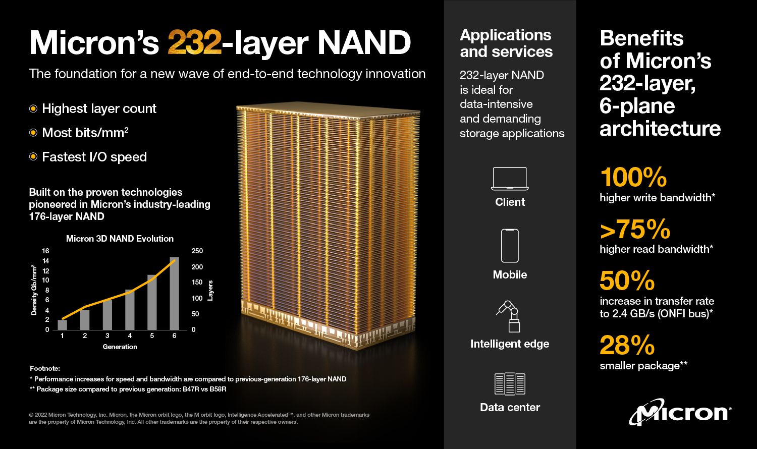
Ahead of next week’s Flash Memory Summit, Micron this morning is announcing that their next-generation 232 layer NAND has begun shipping. The sixth generation of Micron’s 3D NAND technology, 232L is slated to offer both improved bandwidth and larger die sizes – most notably, introducing Micron’s first 1Tbit TLC NAND dies, which at this point are the densest in the industry. According to the company, the new NAND is already shipping to customers and in Crucial SSD products in limited volumes, with further volume ramping to take place later in the year.
Micron first announced their 232L NAND back in May during their Investor Day event, revealing that the NAND would be available this year, and that the company intended to ramp up production by the end of the year. And while that yield ramp is still ongoing, Micron’s Singapore fab is already capable of producing enough of the new NAND that Micron is comfortable in announcing it is shipping, albeit clearly in limited quantities.
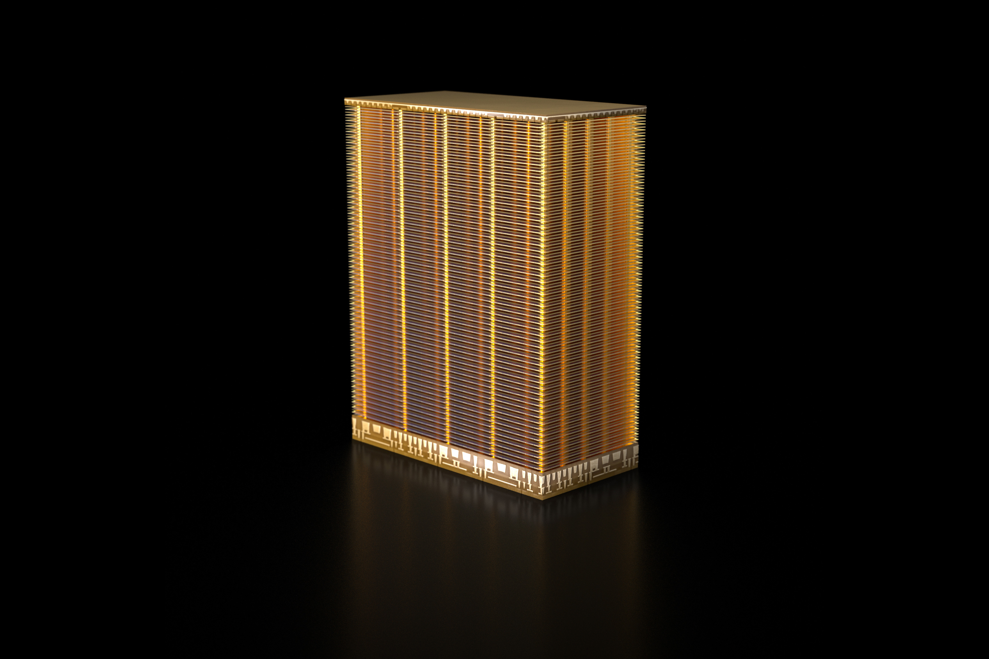
From a technical perspective, Micron’s 232L NAND further builds upon the basic design elements Micron honed in that generation. So we’re once again looking at a string stacked design, with Micron using a pair of 116 layer decks, up from 88 layers in the previous generation. 116 layer decks, in turn, are notable as this is the first time Micron has been able to produce a single deck over 100 layers, a feat previously limited to Samsung. This in turn has allowed Micron to produce cutting-edge NAND with just two decks, something that may not be possible for much longer as companies push toward designs with over 300 total layers.
Micron’s NAND decks continue to be built with their charge-trap, CMOS under Array (CuA) architecture, which sees the bulk of the NAND’s logic placed under the NAND memory cells. Micron has long cited this as giving them an ongoing advantage in NAND density, and that’s once again on show for their 232L NAND. According to the company they’ve achieved a density of 14.6 Gbit/mm2, which is about 43% denser than their 176L NAND. And, according to Micron, anywhere between 35% to 100% denser than competing TLC products.
| Micron 3D TLC NAND Flash Memory | ||
| 232L (B58R) |
176L (B47R) |
|
| Layers | 232 | 176 |
| Decks | 2 (x116) | 2 (x88) |
| Die Capacity | 1 Tbit | 512 Gbit |
| Die Size (mm2) | ~70.1mm2 | ~49.8mm2 |
| Density (Gbit/mm2) | 14.6 | 10.3 |
| I/O Speed | 2.4 MT/s (ONFi 5.0) |
1.6 MT/s (ONFI 4.2) |
| Program Throughput | ? | ? |
| Planes | 6 | 4 |
| CuA / PuC | Yes | Yes |
The improved density has allowed Micron to finally produce their first 1Tbit TLC die, which from a productization standpoint means that Micron can now also produce 2TB chip packages by stacking 16 of their 232L dies. This is good news for SSD capacities, which at the high-end are often limited by the number of packages that can be placed. Though it does mean that there’s a potential loss of performance at lower capacities due to a decrease parallelism from implementing fewer packages.
At the same time, Micron has also been working on the size of their chip packaging, and as a result while the larger capacity means that their die size has increased on a generational basis (we estimate ~70.1mm2 given Micron’s density figures), they’ve still shrunk their chip packaging by 28%. As a result, a single chip package is down from 12mm x 18mm (216mm2) to 11.5mm x 13.5mm (~155mm2). So for Micron’s downstream customers, the combination of the greater capacity and physically smaller packages for Micron’s NAND means that device manufacturers can cut down on the amount of space they allocate to NAND packages, or go the other direction and try to cram in even more packages into a similar amount of space.
Besides density improvements, the latest generation of Micron’s NAND is also allowing the company to upgrade their hardware to take advantage of newer I/O technologies, as well as to implement their own improvements to increase transfer speeds. The big news here is that Micron has increased the number of planes within their NAND die from 4 to 6, further improving the parallelism available within each die. Quad (four) plane designs became common in the previous generation of NAND, and as the density of NAND grows, so too are the number of planes in order for transfer rates to keep up with these greater densities. Micron has confirmed that the planes in 232L NAND offer independent reads, though they aren’t being quite as explicit on what kind of wordline dependencies remain for writes.
This increase in parallelism, along with improved internal transfer rates, has allowed Micron to significantly improve their per-die read and write speeds. According to the company, read speeds have improved by over 75% over their 176L generation NAND, and meanwhile write speeds have outright doubled.
Coupled with this, Micron has also implemented the latest generation of ONFi on their peripheral logic. Finalized in 2021 and now rolling out in the first NAND products, ONFi increases controller-NAND transfer rates by 50%, bringing it to 2400MT/second. ONFi 5.0 also introduced a new NV-LPDDR4 signaling method, which is available with the same 2400MT/s rate but, as it’s based on LPDDR technology, consumes less power. According to Micron, they’re seeing per-bit energy transfer savings of over 30%, which makes for a significant reduction in energy consumption. Though as always with these sorts of comparisons, it’s worth noting that the bandwidth gains exceed the energy savings (50% vs. 30%), so our expectation is that overall energy consumption is going to go up for high-performance products that run at the fastest speeds supported by Micron’s 232L NAND.
As for productization, Micron is pitching 232L NAND as a full stack replacement for 176L NAND – meaning that Micron considers it suitable for everything from mobile and IoT to clients and data center products. To that end, the company is already making initial shipments to their customers, including their own Crucial subsidiary. As with past generations of Micron NAND, starting early with Crucial allows the company to get some hands-on experience in developing full-featured products with their new NAND before they roll it into their own enterprise equipment. Interestingly, however, Micron isn’t announcing any new Crucial products right now, which strongly implies that Crucial is going to begin implementing the new NAND in existing products. If that’s the case, then Crucial customers will want to pay attention to what’s going on and what revision of a drive they’re buying, as the larger 1Tb die could have performance implications for products originally designed around 512Gbit dies.
Wrapping things up, today’s announcement should be the tip of the iceberg for Micron’s 232L shipments. With volume ramping expected to continue through this end of this calendar year, Micron’s plans call for the company to significantly increase the amount of next-generation NAND they’re shipping, going well beyond these initial volumes. Ultimately, this means that products equipped with 232L NAND are going to be relatively sparse for this year, and will pick up in 2023 following the volume ramp. So while Micron’s 232L NAND is indeed shipping, from a consumer standpoint we’re likely still several months off (or more) from seeing it becoming a common fixture in SSDs and other products.
Source: Micron


17 Comments
View All Comments
andychow - Tuesday, July 26, 2022 - link
I get what layers mean, but what does plane? 232 isn't divisible by 6, so it can't mean that you can read or write on a 1/6th of a layer without reading all of it. If someone could ELI5 I'd appreciate it.yankeeDDL - Wednesday, July 27, 2022 - link
I asked myself the same question. I don't have the answer but I thought that parity/redundant bits are included in the stack.blanarahul - Monday, August 1, 2022 - link
Think of it like pizza. 176 layer die is a pizza with 4 slices and 232 layer die is a pizza with 6 slices. If you're not allowed to further divide each slice, only 4 people can simultaneously eat pizza in 176 layer die but 6 people can eat pizza in 232 layer die. Hence, 232 is faster.Wereweeb - Tuesday, August 2, 2022 - link
Layers and decks refer to the manufacturing process, where a deck consists of a certain number of layers. Both are stacked horizontally on top of each other.A plane is a vertical subdivision of the whole die, part of the control architecture, and relates to how the NAND die communicates with the SSD's controller. Simply put, each plane is a semi-autonomous subdivision of the NAND die that can be accessed in parallel to some extent (I forget to which extent).
Every storage/memory device is divided and then further sub-divided to make accessing it easier for it's controller. DDR5 has channels, sub-channels, dies, and then the die itself is divided into bank groups, banks, rows and columns, etc...
In this case I think that the NAND planes are best compared to DRAM's bank groups and banks. Both allow for increased parallelization in the larger and denser dies that we're getting by increasing the number of transistors in the control circuitry.
Silver5urfer - Tuesday, July 26, 2022 - link
Micron's 176L NAND is not a joke. It destroys all other NAND technologies out of water. Period. How one might ask.Look at the latest Seagate Firecuda SSDs, they use Micron 176L NAND Flash technology and they are fastest of all, the Firecuda 530 NVMe PCIe4.0 SSD is the fastest. But wait, the thing is not that which actually made me think how Micron is really pushing forth, look at the endurance of the drives which are using that on Seagate.
Samsung 980Pro / SK Hynix Platinum P41 / WD SN850 all of these have exact same damn rating and same capacity limits, at 1200TBW maxed out. 2TB only.
Micron 176L Firecuda 530 at 4TB and the endurance rating at sky high levels it's higher than Samsung MLC 860 Pro 4TB older MLC Samsung V NAND is 4800TBW and the 176L TLC is 5100TBW they beat Samsung MLC with TLC technology. 2TB Firecuda 530 has 2550TBW, that is 2x of the usual WD / SKHynix 2TB drives.
A massive shame is how blisteringly expensive their 530 4TB NVMe SSD is. I guess once PCIe 5.0 comes out they will make this cheaper, I hope so. I can finally grab a couple of these and replace my brand new 980 Pros (use them as USB C drives).
Samsung still did not create any meaningful alternative to their MLC technology in Endurance at all, pathetic really how far they have hamstrung their own leadership technology for BS profit maximization. Their LSI fabrication of 8N (Ampere Nvidia exclusive) is also a mere small step from their 10nm. GDDR6 finally caught up with Micron PAM4 GDDR6X though. But Micron probably is efficient now.
Where's SanDisk ? After being brought out by WD, they failed hard. I do not see their SanDisk Extreme Pro series anymore it was the only drive along with Samsung 850 Pro to have 10 Year warranty, the last MLC drives. And also KIOXIA being a pet of Bain capital (WD, Apple and Toshiba) they fell flat on face in sheer innovation now.
But the biggest failure is on Intel, their greedy pig investors were happy pumping the money and using it to siphon off made a ton of cash on x86 and dumped it with Apple being their new child. Result ? R&D axed off totally, 3DXPoint dead, the best of Human technology in Memory now buried. Look at the Intel Optane P5800X and see the Endurance and bandwidth on that beast. RIP Optane / 3DXpoint.
I hope the BS PLC doesn't see light and we see more endurance and performance from TLC itself.
Chaser - Tuesday, July 26, 2022 - link
"Look at the latest Seagate Firecuda SSDs, they use Micron 176L NAND Flash technology and they are fastest of all, the Firecuda 530 NVMe PCIe4.0 SSD is the fastest."The Hynix P41 is the fastest SSD today.
A5 - Wednesday, July 27, 2022 - link
Unless you have specific workloads, the drive will be obsolete before you get anywhere near that 1200TBW, much less 2550TBW.My 8 year-old 840 EVO is still at 90-something percent of its p/e cycles remaining.
romrunning - Wednesday, July 27, 2022 - link
(sigh) I continue to lament Optane's passing. What a performer! If both Micron & Intel had kept at it, they could have made it less expensive. Instead, more lost R&D and manufacturing just because the first few iterations weren't instant profit leaders.nandnandnand - Wednesday, July 27, 2022 - link
Several other companies have been working on competitors to Optane, even before it launched. HP's vaporware memristors, Crossbar ReRAM, poorly named Storage Class Memory (IBM?), MRAM, and inferior flash-based alternatives like Toshiba XL-Flash, Samsung Z-NAND, etc.Some of these could take Optane's place, but ultimately we want a universal memory that can replace both DRAM and NAND. Optane was not it and did not live up to its initial hype.
Wereweeb - Tuesday, August 2, 2022 - link
No one wants universal memory. I want a low latency non-volatile memory to replace some SRAM and all DRAM (MRAM fits the bill) and I want a cheap rewriteable memory to replace NAND when it stops shrinking (Whatever can be easily stacked into hundreds of layers). Both of these goals are at odds with eachother, since designing and fabbing a memory always involves tradeoffs.